Semiconductor device and method of manufacturing the same

A device manufacturing method and semiconductor technology, which are applied in the fields of semiconductor/solid-state device manufacturing, semiconductor devices, electrical components, etc., can solve problems such as difficulty in effectively controlling the position and thickness of the barrier layer, and difficulty in effectively controlling the effect of the barrier layer, so as to suppress parasitic trenches. effects of channel and channel punch-through effects, improving device reliability, and simplifying processes

Active Publication Date: 2019-01-18
INST OF MICROELECTRONICS CHINESE ACAD OF SCI
View PDF6 Cites 0 Cited by
  • Summary
  • Abstract
  • Description
  • Claims
  • Application Information

AI Technical Summary

Problems solved by technology

However, this process requires additional implantation steps and it is difficult to effectively control the position and thickness of the barrier layer, as well as properties such as the doping concentration of the doped barrier layer, making it difficult to effectively control the effect of the barrier layer

Method used


Image

  • Semiconductor device and method of manufacturing the same
  • Semiconductor device and method of manufacturing the same
  • Semiconductor device and method of manufacturing the same

Examples


Embodiment Construction

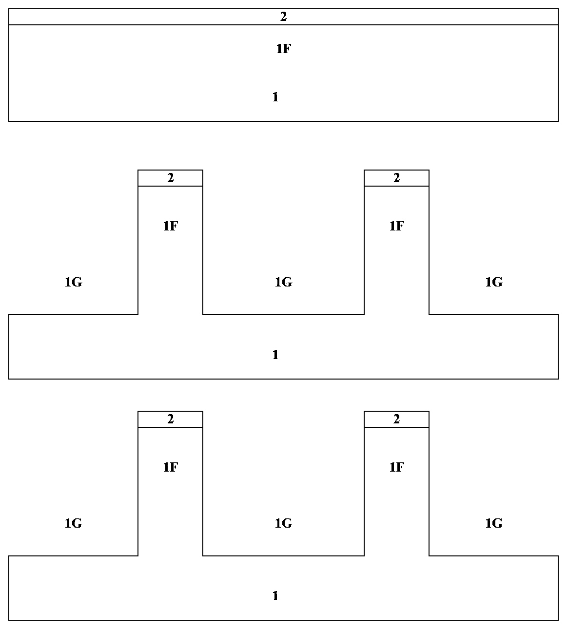
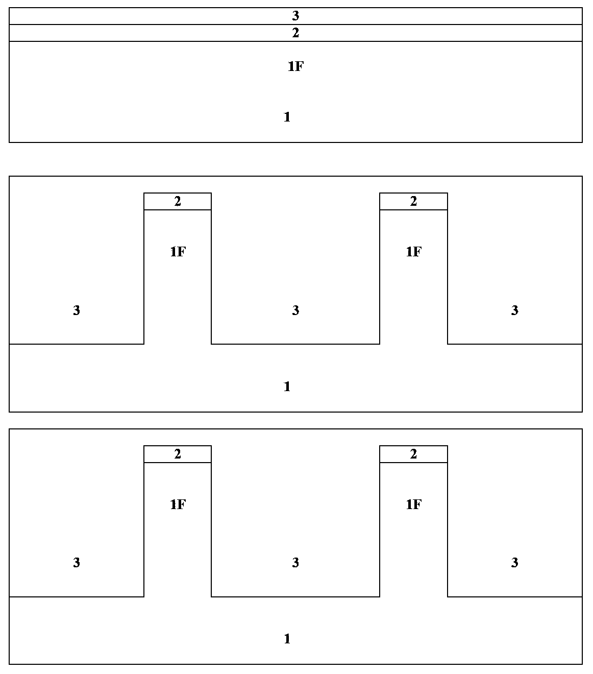
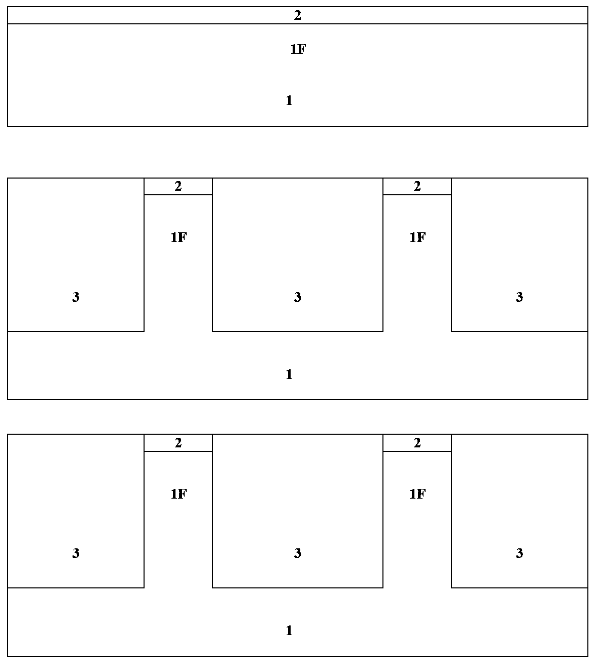
[0021] The features and technical effects of the technical solution of the present invention will be described in detail below with reference to the accompanying drawings and in combination with schematic embodiments, and a three-dimensional multi-gate FinFET capable of effectively suppressing parasitic channel effects and a manufacturing method thereof are disclosed. It should be pointed out that similar reference numerals represent similar structures, and the terms "first", "second", "upper", "lower" and the like used in this application can be used to modify various device structures or manufacturing processes . These modifications do not imply spatial, sequential or hierarchical relationships of the modified device structures or fabrication processes unless specifically stated.

[0022] It is worth noting that the upper part of each of the following figures is the device along the Figure 16 The cross-sectional view of the first direction (fin extension direction, source-...


PUM


Abstract

The invention discloses a semiconductor device and a manufacturing method thereof. The semiconductor device comprises a plurality of fins disposed on a substrate and extending along a first direction, a shallow trench isolation disposed between the fins, and a punch-through barrier layer disposed at an interface between the fins and the top of the shallow trench isolation. According to the semiconductor device and the manufacturing method thereof of the invention, a heavily doped sacrificial isolation layer is utilized on the fins, and a uniform and steep punch-through barrier layer is formed through diffusion at the bottom of the fins, which effectively restrains the parasitic channel effect and the channel punch-through effect, simplifies the process, and improves the reliability of the device.

Description

technical field [0001] The invention relates to a semiconductor device and a manufacturing method thereof, in particular to a three-dimensional multi-gate FinFET capable of effectively suppressing parasitic channel effects and channel penetration effects and a manufacturing method thereof. Background technique [0002] In the current sub-20nm technology, the three-dimensional multi-gate device (FinFET or Tri-gate) is the main device structure, which enhances the gate control ability and suppresses leakage and short channel effects. [0003] For example, compared with traditional single-gate bulk Si or SOI MOSFETs, MOSFETs with double-gate SOI structures can suppress short-channel effects (SCE) and drain-induced barrier lowering (DIBL) effects, have lower junction capacitance, and can To achieve light channel doping, the threshold voltage can be adjusted by setting the work function of the metal gate, which can obtain about 2 times the driving current and reduce the requireme...

Claims


Application Information

Patent Timeline
Patent Type & Authority Patents(China)
IPC IPC(8): H01L21/336H01L29/78H01L29/06
Inventor 殷华湘陈率朱慧珑
Owner INST OF MICROELECTRONICS CHINESE ACAD OF SCI
Why Eureka
Try Eureka