Method and device for firmly welding smd nuts on printed circuit boards
A printed circuit board and nut technology, applied in the direction of assembling printed circuits with electrical components, can solve problems such as the inability to meet the requirements of product reliability testing, and achieve the effects of long service life, firm connection, and prevention of falling off
- Summary
- Abstract
- Description
- Claims
- Application Information
AI Technical Summary
Problems solved by technology
Method used
Image
Examples
Embodiment 1
[0022] A method for firmly welding SMD nuts on a printed circuit board. The first step is to cut the nut steel mesh. The area of the nut steel mesh is larger than the contact surface between the nut and the PCB board. The second step is to open holes on the nut steel mesh and open the nut legs. Pillar hole, the radius of the hole of the nut stencil is smaller than the radius of the hole on the PCB, the third step is to install the nut stencil, brush the solder paste, and then paste the SMD nut on the pad coated with solder paste, because The radius of the nut steel mesh is smaller than the opening radius of the post hole on the PCB. When the nut is attached to the pad coated with solder paste, a little solder paste will be attached to the post. The fourth step is through reflow soldering, at a high temperature of 220-250°C Under the environment, the solder paste is melted, and the excess solder paste flows along the hole of the column foot. After the alloy composition is cool...
Embodiment 2
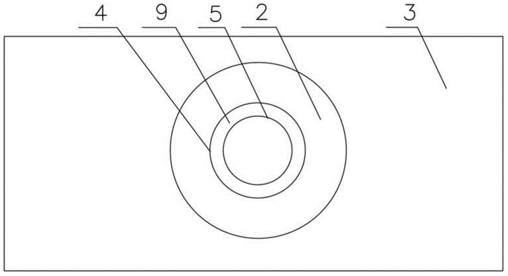
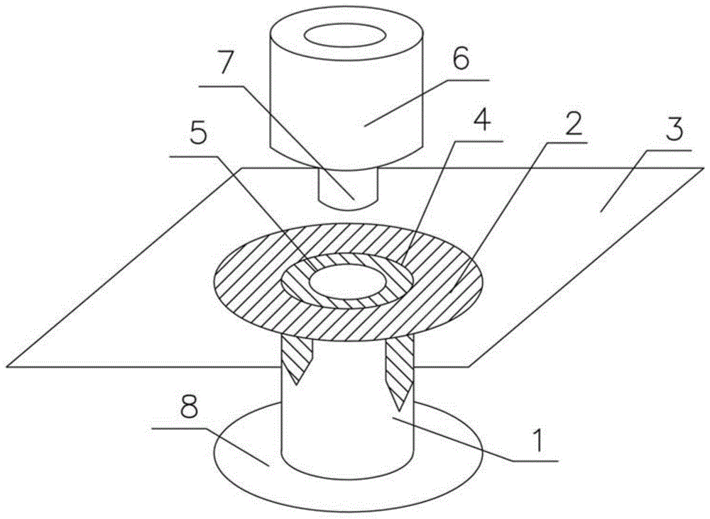
[0024] A device for firmly welding SMD nuts on a printed circuit board, comprising: a nut leg, the nut leg is connected to a nut steel mesh 2, and both the nut leg and the nut steel mesh are connected to a PCB Board 3, opening 5 on the nut stencil, opening 4 on the nut stencil, the radius of the hole on the nut stencil is smaller than the radius of the sill hole on the PCB, inserting the nut into the stencil hole The post 7 of 6, the nut is connected to the BOT surface of the PCB through the hole on the PCB.
[0025] attached image 3 The entire shadow plane is the nut steel mesh. After being heated, the solder paste flows through the hole 5 and flows into the inner wall of the pcb column foot hole 4. image 3 Part number 1 is a three-dimensional view of the PCB opening, which is the through hole used when the pin is inserted into the PCB.
Embodiment 3
[0027] The device for firmly welding the SMD nut described in embodiment 2 on a printed circuit board, the outer diameter of the nut is 3.15-3.25mm, the height is 3.00-3.05mm, and the diameter of the post is 1.97-2.00mm , the height is 0.60-0.65mm.
PUM
 Abstract
Description
Claims
Application Information


