
Method for flattening through-silicon-via back-surface metal

A planarization method and a technology of penetrating silicon vias, which are applied in the fields of electrical components, semiconductor/solid-state device manufacturing, circuits, etc., and can solve problems such as weak mechanical strength of the dielectric layer, affecting the electrical performance of the through hole, and damage to the dielectric layer

Active Publication Date: 2014-11-12
ACM RES SHANGHAI
View PDF3 Cites 1 Cited by
  • Summary
  • Abstract
  • Description
  • Claims
  • Application Information

AI Technical Summary

Problems solved by technology

However, no matter which of the above methods will generate strong mechanical stress, and the dielectric layer around the through hole has weak mechanical strength, it is easy to cause damage to the dielectric layer on the shoulder of the through hole during grinding or cutting. Defects are generated, which in turn affect the electrical performance of the through hole, reducing the performance and life of the packaged integrated circuit

Method used


Image

  • Method for flattening through-silicon-via back-surface metal
  • Method for flattening through-silicon-via back-surface metal
  • Method for flattening through-silicon-via back-surface metal

Examples


Embodiment Construction

[0017] In order to describe the technical content, achieved goals and effects of the present invention in detail, the following will be described in detail in conjunction with the embodiments and accompanying drawings.

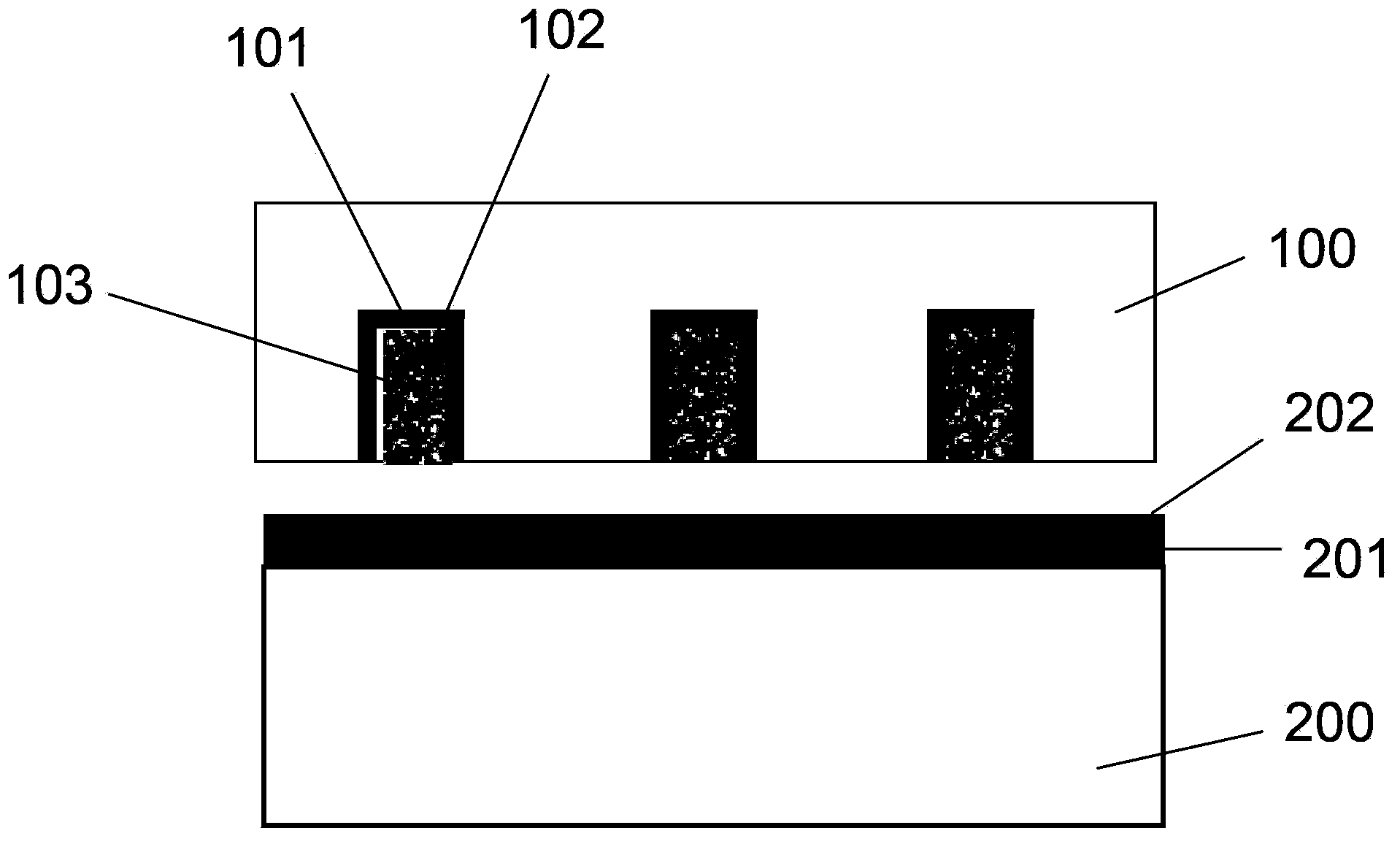
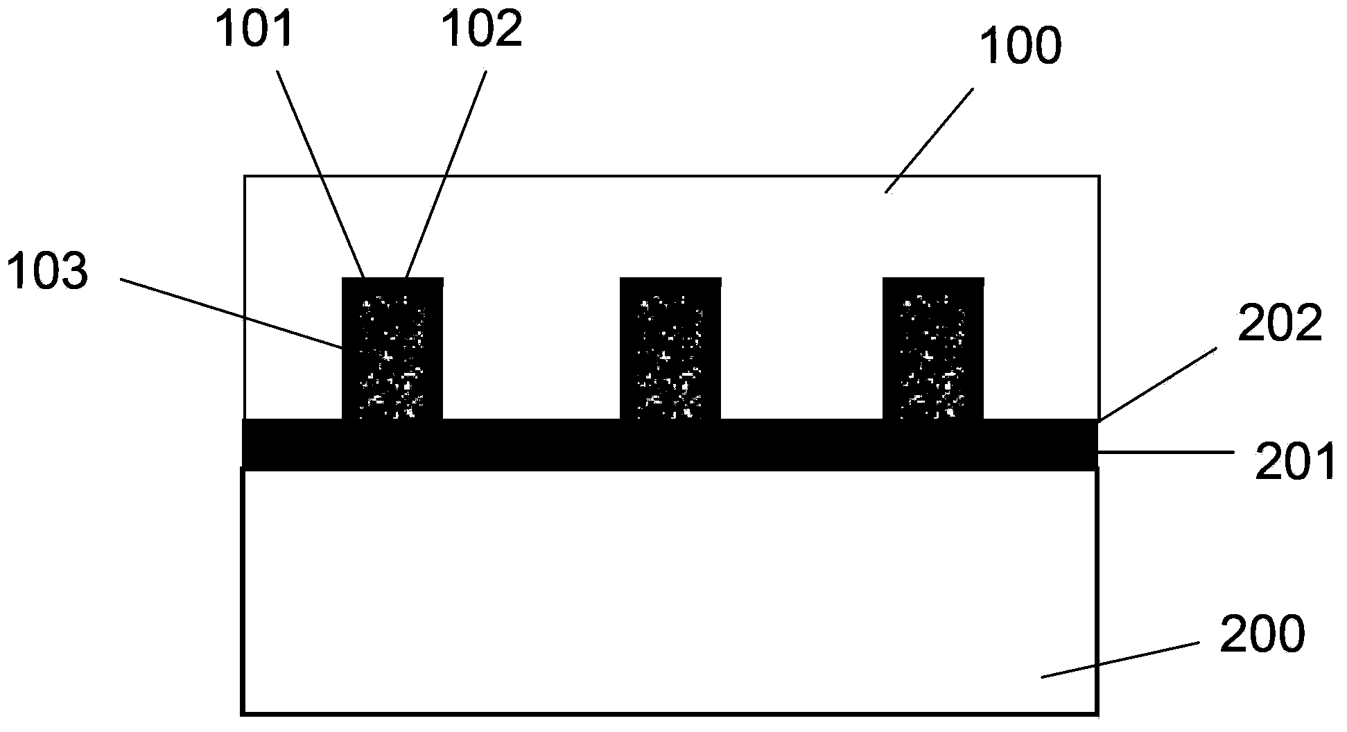
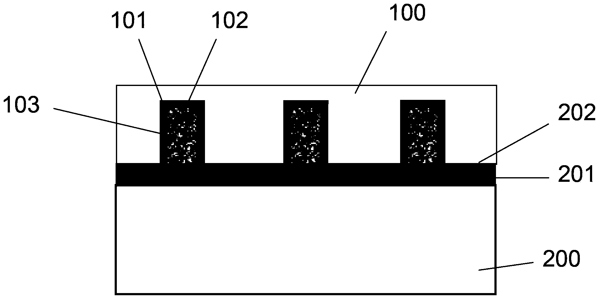
[0018] Before detailing the method for planarizing the metal on the back of the TSV of the present invention, the disclosure of the metal on the back of the TSV will be described first. After the metal on the back of the TSV is exposed, the metal on the back of the TSV is flattened by using the present invention, so that the metal on the back of the TSV is flush. The metal exposure method on the back side of the TSV is not limited to the following method, and the following method is only described as a representative embodiment.

[0019] refer to Figures 1 to 8B The method for exposing the metal on the backside of the TSV includes the following steps:

[0020] First, if figure 1 As shown, a silicon substrate 100 and a carrier sheet 200 are provided. The s...


PUM


Abstract

The invention discloses a method for flattening through-silicon-via back-surface metal. The method comprises the steps that a silicon substrate with a plurality of metal protrusions exposed out of the back surface of the silicon substrate is provided; the metal protrusions exposed out of the back surface of the silicon substrate are flattened through the unstressed electrochemical polishing method so as to be flush. According to the method, the metal protrusions exposed out of the back surface of the silicon substrate are flattened through the unstressed electrochemical polishing method, the thickness of the removed portions of the metal protrusions can be accurately controlled by controlling the polishing voltage and / or current or the rotation speed and the horizontal movement speed of the silicon substrate, and therefore the metal protrusions on the back surface of the silicon substrate can be flattened.

Description

technical field [0001] The invention relates to the technical field of semiconductor integrated circuit manufacturing, in particular to a metal planarization method on the back side of a through-silicon hole. Background technique [0002] With the continuous development of electronic complete systems in the direction of lightness, thinness, and smallness, the requirements for the integration level of integrated circuits are also getting higher and higher. At present, improving the integration of integrated circuits is mainly to reduce the feature size, so that more components can be integrated in a given area, which belongs to two-dimensional integration. However, as the structure of integrated circuits becomes increasingly complex and the required functions become increasingly powerful, the limitations of the application of two-dimensional integration technology are gradually highlighted. Therefore, new integration technologies need to be sought to improve the integration ...

Claims


Application Information

Patent Timeline
IPC IPC(8): H01L21/768
CPCH01L21/7684H01L21/76898
Inventor 王坚贾照伟金一诺王晖
Owner ACM RES SHANGHAI
Learn More