Method for manufacturing pairing marks of CF substrate

A production method and group marking technology, which is applied in the direction of instruments, nonlinear optics, optics, etc., can solve the problems of low recognition of materials, only leftovers, and inability to provide clear alignment references in the process, so as to improve recognition and improve optical quality. effect of density

Active Publication Date: 2014-11-19
TCL CHINA STAR OPTOELECTRONICS TECH CO LTD
View PDF6 Cites 8 Cited by
  • Summary
  • Abstract
  • Description
  • Claims
  • Application Information

AI Technical Summary

Problems solved by technology

[0006] But BOA technology also has some problems, such as figure 2 As shown, since the black matrix is ​​fabricated on the TFT substrate in the panel of the BOA structure, only the color resist, the photo spacer (Photo spacer, PS) 200 ′, and the ITO pixel electrode remain on the CF substrate 100 ′ on the other side. And other structures, but lack of high optical density (Optical Density, OD) materials, because the photosensitive coupling detector (Charge Coupled Device, CCD) does not have a high degree of recognition of materials with low optical density, so it cannot be formed on the CF substrate and the traditional structure The same alignment mark on the LCD panel cannot provide a clear alignment reference for subsequent processes

Method used


Image

  • Method for manufacturing pairing marks of CF substrate
  • Method for manufacturing pairing marks of CF substrate
  • Method for manufacturing pairing marks of CF substrate

Examples


Embodiment Construction

[0030] In order to further illustrate the technical processing adopted by the present invention and its effects, the following is a detailed description in conjunction with preferred embodiments of the present invention and accompanying drawings.

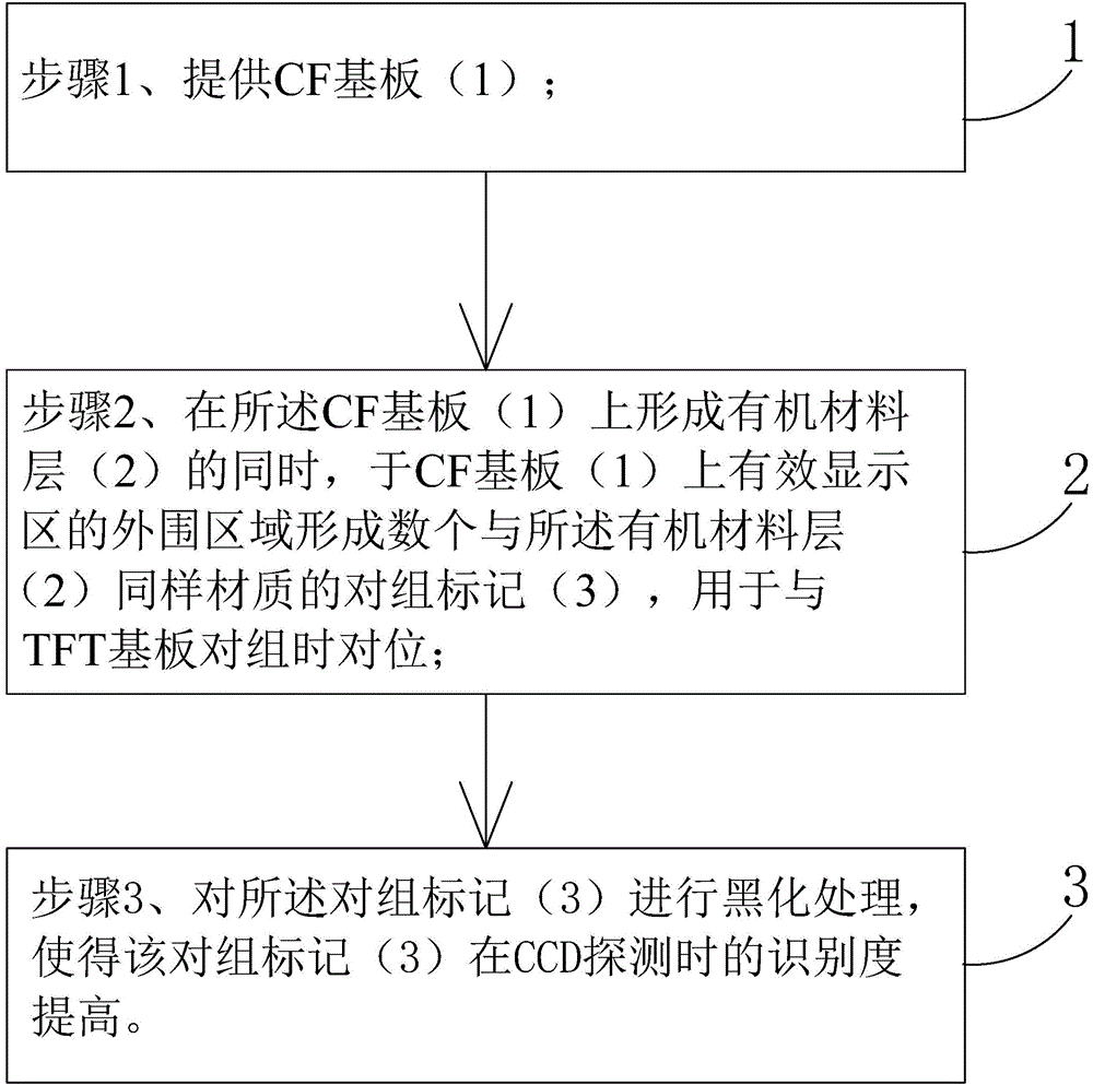
[0031] see Figure 2 to Figure 7 , the present invention provides a method for making a group mark on a CF substrate, comprising the following steps:

[0032] Step 1, providing a CF substrate 1 .

[0033] The CF substrate 1 is a CF substrate in a BOA structure liquid crystal display panel. Since the BOA structure liquid crystal display panel manufactures the black matrix on the TFT substrate, the CF substrate 1 in step 1 does not have materials with high optical density, nor does it have the same group marks as the traditional structure liquid crystal display panel.

[0034] Step 2, such as Figure 4 As shown, while the organic material layer 2 is formed on the CF substrate 1 , several paired marks 3 of the same material as the o...


PUM


Abstract

The invention provides a method for manufacturing pairing marks of a CF substrate. The method comprises the steps that step 1, the CF substrate (1) is provided; step 2, while an organic material layer (2) is formed on the CF substrate (1), multiple pairing marks (3) are formed on the peripheral area of an effective display area of the CF substrate (1) and made of the same material as the organic material layer (2), and the pairing marks (3) are used for achieving counterpoint when the CF substrate is paired with a TFT substrate; step 3, the pairing marks (3) are blackened, so that the recognition degree of the pairing marks (3) in CCD detection is improved. The method can improve the recognition degree of the pairing marks (3) in CCD detection, so that the pairing marks provide precise counterpoint reference for subsequent processing.

Description

technical field [0001] The invention relates to the technical field of liquid crystal display, in particular to a method for manufacturing a group mark of a CF substrate. Background technique [0002] A Liquid Crystal Display (LCD) has many advantages such as thin body, power saving, and no radiation, and has been widely used. Such as: LCD TV, mobile phone, personal digital assistant (PDA), digital camera, computer screen or laptop screen, etc. [0003] Generally, a liquid crystal display device includes a housing, a liquid crystal display panel disposed in the housing, and a backlight module disposed in the housing. Among them, the structure of the liquid crystal display panel is mainly composed of a thin film transistor array substrate (Thin Film Transistor Array Substrate, TFT Array Substrate), a color filter substrate (Color Filter, CF), and a liquid crystal layer ( Liquid Crystal Layer), its working principle is to control the rotation of liquid crystal molecules in t...

Claims


Application Information

Patent Timeline
Patent Type & Authority Applications(China)
IPC IPC(8): G02F1/1335
CPCG02F1/133516G02F1/136209G02F1/133354G02F1/133514
Inventor 熊源连水池
Owner TCL CHINA STAR OPTOELECTRONICS TECH CO LTD
Why Eureka
Try Eureka