

Manufacturing method for curved surface display
A manufacturing method and display technology, applied in the direction of instruments, nonlinear optics, optics, etc., can solve problems such as color shift and affect the image display quality of the device, and achieve the effect of improving the phenomenon of color deviation
- Summary
- Abstract
- Description
- Claims
- Application Information
AI Technical Summary
Problems solved by technology
Method used
Image

Examples
specific Embodiment
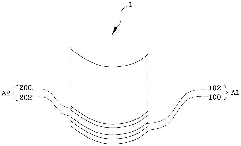
[0033] In a specific embodiment, the manufacturing method further includes: pre-bending the thin film transistor glass 102 so that the curved surface after bending corresponds to the curvature of the shape of the first curved glass 100 . The color filter glass 202 is pre-curved so that the curved surface corresponds to the curvature of the second curved glass 200 . Preferably, the respective curvatures of the first curved glass 100 and the second curved glass 200 are equal.
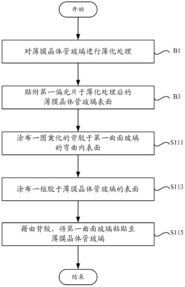
[0034] In a specific embodiment, the manufacturing method further includes: before forming the first component A1, thinning the thin film transistor glass 102 first, and then attaching a first polarizer to the thinned thin film transistor glass 102 surface. In addition, before forming the second component A2 , the color filter glass 202 may be thinned first, and then a second polarizer is attached to the surface of the thinned color filter glass 202 .
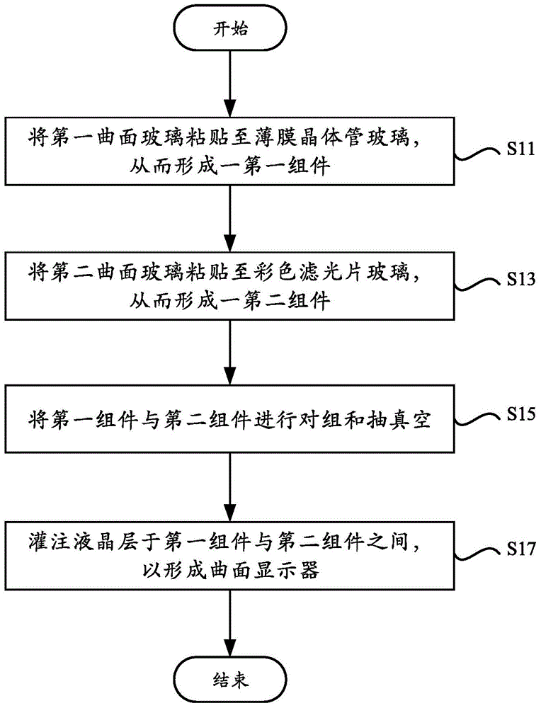
[0035] image 3 shown in figure 2 In the manufa...
PUM
 Abstract
Description
Claims
Application Information