Mold and method for preparing thyristor chip mesa insulation protective layer using it

A technology of insulating protective layer and thyristor, which is applied in semiconductor/solid-state device manufacturing, electrical components, circuits, etc., can solve the problems of chip blocking voltage reduction, thin insulating protective layer, breakdown, etc., to prevent ultra-high voltage breakdown , increase the creepage distance, the effect of high insulation voltage

Active Publication Date: 2017-02-15
NINGBO SILCR POWER SEMICON
View PDF5 Cites 0 Cited by
  • Summary
  • Abstract
  • Description
  • Claims
  • Application Information

AI Technical Summary

Problems solved by technology

However, this preparation method has the following problems: 1) During the preparation process, when the vulcanized silicone rubber is coated to the edge of the chip, it is in a fluid uncured state, so the thickness of the silicone layer after self-flow molding under gravity is generally 0.3-0.4mm, however, the reliable breakdown voltage of a 1mm thick silica gel layer is generally 10000V, which means that the insulating protective layer obtained by this preparation method is more reliable for thyristor chips of 4000V and below 4000V; 2) This preparation method can obtain The shortest creepage distance of the insulation protection layer from the anode edge to the cathode surface is generally 2-4mm. When the humidity or cleanliness of the environment where the chip is located is slightly poor, it is easy to cause ignition due to insufficient surface creepage distance. The insulating protective layer obtained by the preparation method is not suitable for ultra-high voltage thyristor chips of 6500-8500v
To sum up, if the ultra-high voltage thyristor chip is insulated and protected by the insulating protective layer obtained by this preparation method, it is very easy to break down due to the thin insulating protective layer, or to catch fire due to insufficient surface creepage distance of the insulating protective layer. , resulting in a decrease in chip blocking voltage or failure

Method used


Image

  • Mold and method for preparing thyristor chip mesa insulation protective layer using it
  • Mold and method for preparing thyristor chip mesa insulation protective layer using it
  • Mold and method for preparing thyristor chip mesa insulation protective layer using it

Examples


Embodiment Construction

[0020] The present invention will be further described in detail below in conjunction with the accompanying drawings and embodiments.

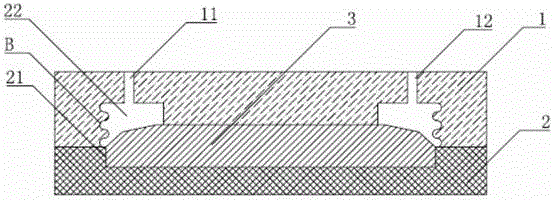
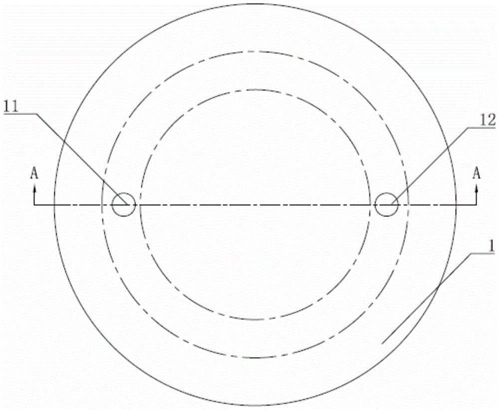
[0021] Such as Figure 1~2 As shown, a mold includes an upper template 1 and a lower template 2 that are made of clean polytetrafluoroethylene plastics and matched, and the lower template 2 is provided with a chip placement groove 21 that can closely cooperate with the thyristor chip 3; The upper part of the upper template 1 is provided with a glue injection hole 11 for injecting glue; the lower part of the upper template 1 is provided with a groove 22 corresponding to the edge table position of the thyristor chip 3 and connected with the glue injection hole 11, as figure 1 The part indicated by the middle dotted line is the edge mesa part of the thyristor chip 3, and the groove wall on the outside of the groove 22 is in a sinusoidal shape (such as figure 2 shown in B), and the height of the groove wall on the outside of the groove 22 is 5 m...


PUM

PropertyMeasurementUnit
heightaaaaaaaaaa
thicknessaaaaaaaaaa
heightaaaaaaaaaa

Abstract

The invention provides a mold and method for preparing an insulating protective layer for a table surface of a thyristor chip with the mold. The mold comprises an upper mold plate and a lower mold plate which are made of high-temperature resistant plastics and are matched with each other, wherein a chip placing groove, which can be in close fit with the chip, is formed in the lower mold plate; a glue injection hole is formed in the upper part of the upper mold plate; a groove, which corresponds to the edge table surface of the chip and is communicated with the glue injection hole, is formed in the lower part of the upper mold plate; the outer groove wall of the groove is curvilinear; when the chip is placed in the chip placing groove, and the upper mold plate and the lower mold plate are tightly pressed on the chip, part of the end surface, corresponding to the chip placing groove, of the bottom end surface of the upper mold plate is clung to the non-edge table surface of the chip, and the edge table surface of the chip seals the groove mouth of the groove to ensure that a glue liquid accommodating cavity is defined by the groove and the edge table surface of the chip. The method has the advantages that the structure is simple; the insulating protective layer of the chip table surface prepared according to a corresponding method is thicker and controllable in thickness, extra-high voltage breakdown can be avoided, the creepage distance is enlarged, and ignition can be avoided.

Description

technical field [0001] The invention relates to an insulation protection method for a thyristor chip mesa, in particular to a mold and a method for preparing an insulation protection layer for a thyristor chip mesa using the mold. Background technique [0002] In the field of high-power and ultra-high-power power control, with the advancement and development of technology, the voltage of electrical equipment is constantly increasing, and the voltage of the thyristors used in it is also constantly increasing. At present, the voltage of ultra-high voltage thyristors in foreign countries has been developed to the level of 7000-8500V. When the internal structure of the chip is normal, the blocking voltage of the thyristor is determined by the breakdown voltage of the chip table, and the breakdown voltage of the chip table is determined by the insulating protective layer of the table. Therefore, for ultra-high voltage thyristors In other words, this requires a very high voltage ...

Claims


Application Information

Patent Timeline
Patent Type & Authority Patents(China)
IPC IPC(8): H01L21/56
Inventor 王大江王森彪徐艳艳李建忠
Owner NINGBO SILCR POWER SEMICON
Why Eureka
Try Eureka