The preparation method of ito film layer and the preparation method of led chip

An LED chip and film technology, applied in coating, metal material coating process, ion implantation plating, etc., can solve the problems of substrate surface damage, poor current impact resistance, poor compactness, etc., to achieve enhanced ohmic contact, The effect of increasing spillover efficiency and improving product quality

Inactive Publication Date: 2017-01-18
ENRAYTEK OPTOELECTRONICS
View PDF7 Cites 0 Cited by
  • Summary
  • Abstract
  • Description
  • Claims
  • Application Information

AI Technical Summary

Problems solved by technology

The E-Beam ITO film layer is composed of multiple ITO polycrystalline grains, the surface is rough and the density is poor, the light scatters and absorbs more inside it, and the current impact resistance is worse than that of RPD ITO and Sputter ITO, therefore, the E-BeamITO film has a tendency to be gradually replaced; the RPD ITO film is denser and the surface is smoother, but the process parameters of the preparation process are relatively simple, and the parameters and structure of the ITO film are not scalable; The Sputter ITO film is denser and has a smoother surface, and ITO films with different refractive indices can be prepared by controlling the process parameters of the film-forming process. It has strong scalability for the preparation of ITO with different properties and structures, and has become more and more popular. Applications
[0004] Magnetron sputtering technology is a process in which plasma bombards the target in a high-vacuum environment so that the target ions overflow and gradually deposit on the GaN substrate. The greater the energy of the plasma bombarding the target, the greater the energy obtained by the target ions. The larger the ITO film, the denser the final ITO film, the better the photoelectric performance and the more resistant to current impact; however, when the energy of the target ions is higher, the bombardment of the substrate when the target ions are deposited on the surface of the substrate to form a film Higher, it is easy to damage the surface of the substrate, which will affect the performance of the device

Method used


Image

  • The preparation method of ito film layer and the preparation method of led chip
  • The preparation method of ito film layer and the preparation method of led chip
  • The preparation method of ito film layer and the preparation method of led chip

Examples


Embodiment Construction

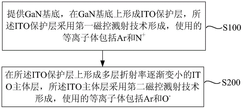
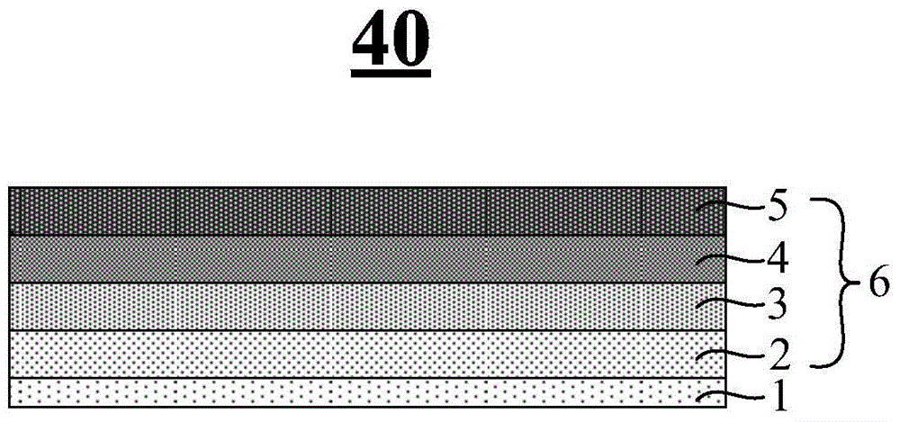
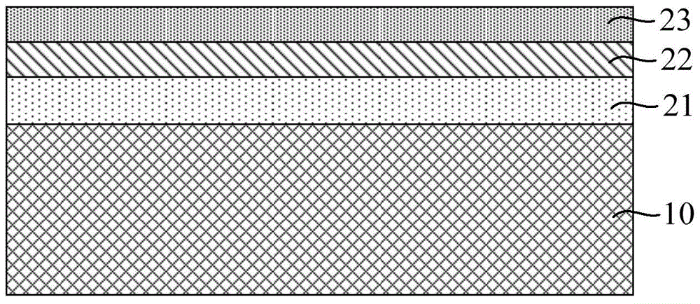
[0029] The preparation method of the ITO film layer of the present invention and the preparation method of the LED chip will be described in more detail below in conjunction with the schematic diagram, wherein a preferred embodiment of the present invention is shown, and it should be understood that those skilled in the art can modify the present invention described here, while still achieving the advantageous effects of the present invention. Therefore, the following description should be understood as the broad knowledge of those skilled in the art, but not as a limitation of the present invention.

[0030] In the interest of clarity, not all features of an actual implementation are described. In the following description, well-known functions and constructions are not described in detail since they would obscure the invention with unnecessary detail. It should be appreciated that in the development of any actual embodiment, numerous implementation details must be worked ou...


PUM

PropertyMeasurementUnit
thicknessaaaaaaaaaa
thicknessaaaaaaaaaa

Abstract

The invention provides an ITO film preparation method and an LED chip preparation method. An ITO protection layer is formed by utilizing a first magnetron sputtering technology; plasma attacking a GaN substrate in the magnetron sputtering process causes N loss of the GaN substrate, the formed ITO protection layer is added with N+, and the N loss can be compensated, thereby eliminating the damage of the plasma on the GaN substrate under a high sputtering power, preventing In or Sn in the ITO film from permeating to the inner portion of the GaN substrate, effectively enhancing ohmic contact between the ITO film and the GaN substrate, and reducing voltage of the formed LED chip. Besides, the ITO main body layer is a film system with gradually-changing refractive index, thereby improving overflow efficiency of the light effectively and improving the quality of the product.

Description

technical field [0001] The invention relates to the field of LED manufacturing, in particular to a method for preparing an ITO film layer and a method for preparing an LED chip. Background technique [0002] A light emitting diode (Light Emitting Diode, referred to as LED) is a semiconductor solid-state light-emitting device, which is made by using the principle of semiconductor P-N junction electroluminescence. LED chips have good photoelectric properties such as low turn-on voltage, small size, fast response, good stability, long life, and no pollution. Therefore, they are widely used in outdoor and indoor lighting, backlighting, display, traffic indication and other fields. [0003] ITO film is widely used in LED chip preparation process due to its excellent photoelectric properties (high transmittance and low resistance). On the one hand, it can improve current spreading, and on the other hand, it can improve ohmic contact. At present, there are three preparation method...

Claims


Application Information

Patent Timeline
Patent Type & Authority Patents(China)
IPC IPC(8): H01L33/00C23C14/35C23C14/08
CPCC23C14/086C23C14/35H01L33/42
Inventor 朱秀山
Owner ENRAYTEK OPTOELECTRONICS
Why Eureka
Try Eureka