Method for manufacturing short-range wireless communication device using flexible circuit board

A flexible circuit board and wireless communication technology, which is applied to the improvement of metal adhesion of insulating substrates, electrical components, near-field transmission systems, etc., can solve the problem that the thickness of short-distance wireless communication devices cannot be made very thin, and achieve good Economic benefits, cost reduction, simple and effective process

Active Publication Date: 2017-09-15
上海蓝沛信泰光电科技有限公司
View PDF4 Cites 0 Cited by
  • Summary
  • Abstract
  • Description
  • Claims
  • Application Information

AI Technical Summary

Problems solved by technology

[0005] However, since the base film of the flexible circuit board has a certain thickness, the thickness of the short-range wireless communication device cannot be made very thin

Method used


Image

  • Method for manufacturing short-range wireless communication device using flexible circuit board
  • Method for manufacturing short-range wireless communication device using flexible circuit board
  • Method for manufacturing short-range wireless communication device using flexible circuit board

Examples


Embodiment Construction

[0046] The following describes the implementation of the present invention through specific specific examples. Those skilled in the art can easily understand other advantages and effects of the present invention from the content disclosed in this specification. The present invention can also be implemented or applied through other different specific embodiments, and various details in this specification can also be modified or changed based on different viewpoints and applications without departing from the spirit of the present invention.

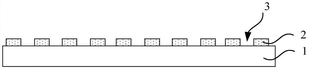
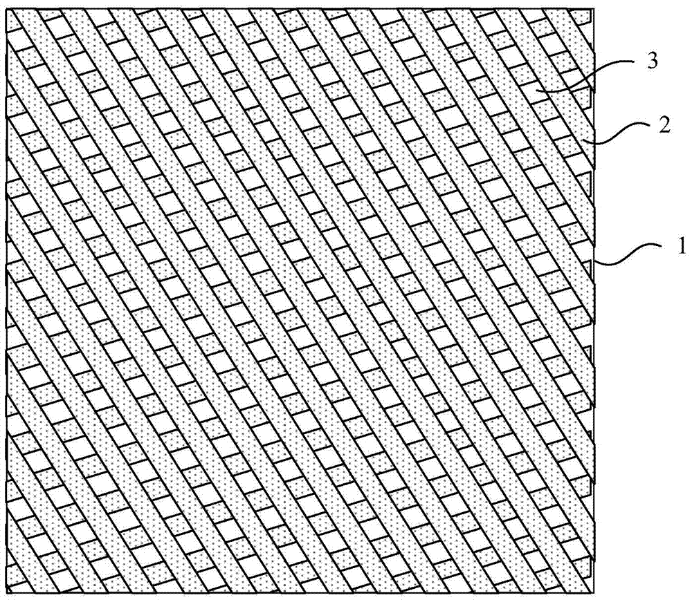
[0047] See Figure 1 to Figure 12 . It should be noted that the illustrations provided in this embodiment only illustrate the basic idea of ​​the present invention in a schematic way, and the figures only show the components related to the present invention instead of the number, shape, and shape of the components in actual implementation. For size drawing, the type, quantity, and proportion of each component can be changed at will during act...


PUM


Abstract

The invention provides a method for manufacturing a NFC (near field communication) device by adopting a flexible circuit board. The method at least comprises the steps as follows: S1: a base membrane is provided, a grid-like connecting material layer is formed in the base membrane; S2: the connecting material layer is coated with expansion adhesive, expansion adhesive particles are formed in the grids, and the connecting material layer and the expansion adhesive particles jointly form an expansion adhesive layer; S3: a copper foil is formed in the surface of the expansion adhesive layer; S4: the copper foil is etched to form a copper circuit; and S5: a slide glass coated with a hot melt adhesive layer is provided, the hot melt adhesive layer is attached to the copper circuit, the expansion particles swell through hot pressing, and the expansion adhesive layer is separated from the copper circuit and the hot melt adhesive layer, so that the copper circuit is left on the hot melt adhesive surface, and the NFC device is formed. According to the method, the ultra-thin NFC device is made with a low cost, has wide application basis and can obtain good economic benefits for an enterprise.

Description

Technical field [0001] The invention belongs to the technical field of short-range wireless communication technology and printed circuit technology, and relates to a method for manufacturing a short-range wireless communication device using a flexible circuit board. Background technique [0002] Near Field Communication (NFC) is a non-contact identification and interconnection technology led by Sony that year; it allows consumer electronics, mobile and smart control tools to perform short-range wireless communication (hereinafter referred to as NFC). ). Sony's lead NFC provides a simple, touch-sensitive solution. [0003] Flexible printed circuit (Flexible Printed Circuit, FPC) has been widely used in connectors or printed circuit boards in various electronic products due to its flexibility. Among various commercially available flexible circuit boards, copper clad laminates are the mainstream products. Generally, the structure of a copper clad laminate includes a polyimide base ...

Claims


Application Information

Patent Timeline
Patent Type & Authority Patents(China)
IPC IPC(8): H05K3/38H04B5/00
Inventor 王庆军杨兆国戴兴根
Owner 上海蓝沛信泰光电科技有限公司
Why Eureka
Try Eureka