Chip removal device

A chip and heating head technology, applied in the direction of electrical components, electrical components, etc., can solve the problems of polarizer burns, over-curing of anisotropic conductive adhesive, etc., and achieve the effects of avoiding burning and curing, reducing scratches, and increasing the contact area

Active Publication Date: 2017-02-15
HEFEI BOE OPTOELECTRONICS TECH +1
View PDF2 Cites 0 Cited by
  • Summary
  • Abstract
  • Description
  • Claims
  • Application Information

AI Technical Summary

Problems solved by technology

[0005] The purpose of the present invention is to provide a chip removal device to solve the technical problems of the prior art that easily cause burns on the polarizer and excessive curing of the anisotropic conductive adhesive when removing the drive chip on the display panel

Method used


Image

  • Chip removal device
  • Chip removal device
  • Chip removal device

Examples


Embodiment Construction

[0024] Specific embodiments of the present invention will be described in detail below in conjunction with the accompanying drawings. It should be understood that the specific embodiments described here are only used to illustrate and explain the present invention, and are not intended to limit the present invention.

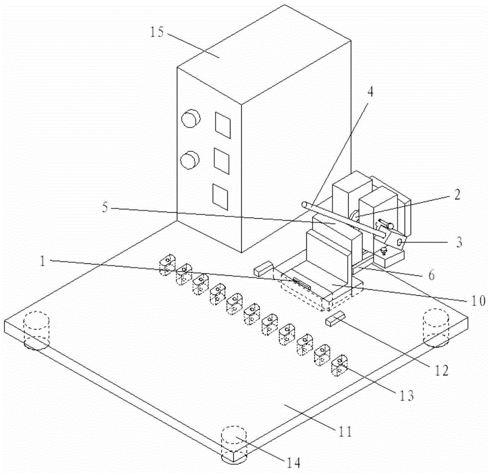
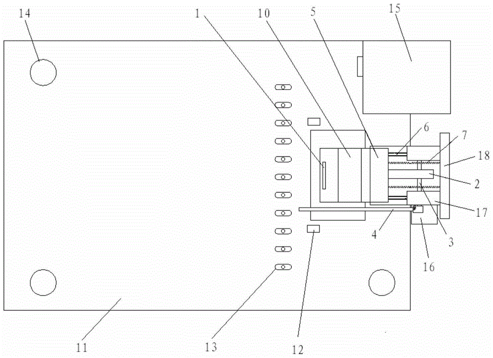
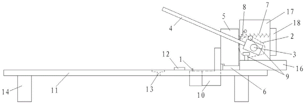
[0025] The invention provides a chip removing device, which is used for removing a chip attached to a display panel, where the chip mainly refers to a drive chip (Drive Integrated Circuit).

[0026] figure 1 is a perspective view of the device, figure 2 and image 3 Top and side views of the device, respectively. The chip removing device includes a heating head 1 for heating the chip. Figure 4 and Figure 5 These are two embodiments of the heating head 1 in the present invention. The heating head 1 includes at least two inner surfaces 101, the two inner surfaces 101 are adjacent or oppositely arranged, and the two inner surfaces 101 are respectively used ...


PUM


Abstract

The invention discloses a chip removing device which is used for removing a chip attached on a display panel, and relates to the field of display panel manufacture. The device comprises a heating head used for heating the chip, wherein the heating head comprises at least two inner side surfaces; the two inner side surfaces are arranged in an adjacent or opposite manner, and are respectively used for being in contact with two adjacent or opposite outer side surfaces of the chip. The device further comprises a driving mechanism which is used for driving the heating head to move in a preset range, and when the heating head moves, the chip can be separated from the display panel. According to the chip removing device, the shape of the heating head is improved, the contact area of the chip and the high temperature heating head is enlarged, the chip is heated uniformly, and burn and solidification of aeolotropic conductive adhesive due to overhigh local temperature are avoided. Besides, the driving mechanism is adopted to achieve the purpose of accurately controlling the moving distance of the heating head, and scald by a polarizer when the display panel is manually displaced to remove the chip is avoided.

Description

technical field [0001] The invention relates to the field of manufacturing display panels, in particular to a chip removing device. Background technique [0002] During the manufacturing process of the display panel, it is necessary to attach a drive chip (Drive Integrated Circuit) to the display panel through an anisotropic conductive glue (ACF), so as to realize the display function of the display panel. However, in the actual production process, there may be defects such as dislocation and damage in the attachment of the chip. At this time, the chip needs to be removed for repair. [0003] The existing chip removal method is to heat the chip to soften the anisotropic conductive adhesive in the corresponding part, and then manually push the display panel to remove the chip. Due to unstable manual force, it is easy to cause the display panel to move excessively, causing the polarizer to come into contact with the high-temperature heating head and cause burns. [0004] In ...

Claims


Application Information

Patent Timeline
Patent Type & Authority Patents(China)
IPC IPC(8): H05K13/04
Inventor 侯永康蔡光源杨建磊张宇
Owner HEFEI BOE OPTOELECTRONICS TECH
Why Eureka
Try Eureka