Integrated structure of optical fiber provided with label-free optical sensing element on one end face and microfluid
A microfluidic structure and optical sensing technology, applied in the field of biosensors, can solve the problems that no one has proposed the integration of sensing elements and microfluidic channels, and achieve the effect of simple structure, short diffusion distance and less usage
- Summary
- Abstract
- Description
- Claims
- Application Information
AI Technical Summary
Problems solved by technology
Method used
Image
Examples
Embodiment 1
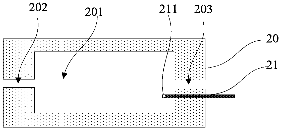
[0033] Such as Figure 1 ~ Figure 2 As shown, the present embodiment provides a fiber end-face marker-free optical sensing element and microfluidic integrated structure, including at least:
[0034] microfluidic structure 20;
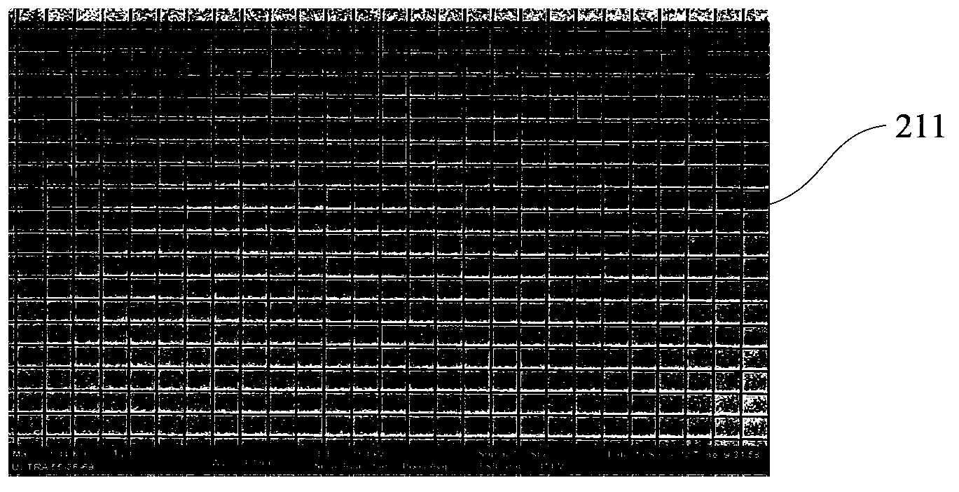
[0035] At least one end face of the optical fiber 21 has an unmarked optical sensing element 211 , and one end of the optical fiber 21 with an unmarked optical sensing element 211 is inserted into the microfluidic frame.
[0036] As an example, the microfluidic structure 20 at least includes a microfluidic channel 201 , a microfluidic inlet 202 and a microfluidic outlet 203 , and of course, the microfluidic structure 20 also has at least one through hole for inserting an optical fiber. Wherein, the microfluidic structure 20 can be prepared by methods such as mold inversion, laser cutting, and micro-nano processing.
[0037] Further, the shape of the microfluidic channel 201 is cylindrical, polygonal columnar or rounded polygonal columnar. Of course, th...
Embodiment 2
[0046] Such as Figure 3 to Figure 9 As shown, this embodiment provides a method for fabricating an optical fiber end-face marker-free optical sensing element and a microfluidic integrated structure, which at least includes the following steps:
[0047] Such as Figure 3 ~ Figure 6 As shown, step 1) is first performed to form a polymer structure 104 having at least one flat surface, a microfluidic groove 105 and at least one linear groove 106 connected to the microfluidic groove 105 in the flat surface.
[0048] As an example, step 1) consists of the following steps:
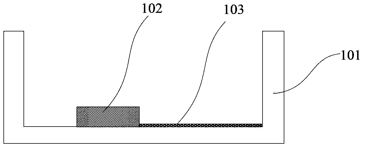
[0049] Such as image 3 As shown, step 1-1) is carried out first, a container 101 with a flat bottom is provided, and a solid block 102 with a predetermined shape and at least one line structure 103 connected with the solid block 102 are fixed at the bottom of the container 101 , the size and shape of the line structure 103 is consistent with that of the optical fiber.
[0050] Such as Figure 4 shown, and ...
PUM
| Property | Measurement | Unit |
|---|---|---|
| width | aaaaa | aaaaa |
| thickness | aaaaa | aaaaa |
| width | aaaaa | aaaaa |
Abstract
Description
Claims
Application Information


