Non-linear photoconductive semiconductor switch testing device and method

A non-linear optical and switch testing technology, applied in the direction of testing dielectric strength, circuit breaker testing, etc., can solve the problems of uneven quality of switches, expensive switches, lack of detection devices, etc.

Inactive Publication Date: 2014-11-26
INST OF FLUID PHYSICS CHINA ACAD OF ENG PHYSICS
View PDF4 Cites 4 Cited by
  • Summary
  • Abstract
  • Description
  • Claims
  • Application Information

AI Technical Summary

Problems solved by technology

[0004] At present, the production process of domestic nonlinear photoconductive switches is not yet mature. On the one hand, the switch is expensive, on the other hand, the quality of the switch is

Method used


Image

  • Non-linear photoconductive semiconductor switch testing device and method
  • Non-linear photoconductive semiconductor switch testing device and method
  • Non-linear photoconductive semiconductor switch testing device and method

Examples


Embodiment 1

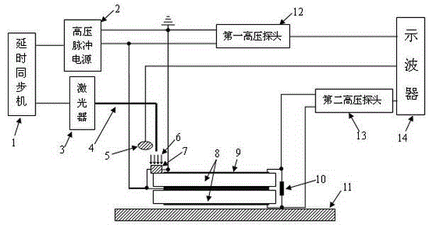
[0068] Embodiment 1: Testing the turn-on delay time of the nonlinear photoconductive switch to be tested , the jitter of the nonlinear photoconductive switch to be tested And the on-resistance of the nonlinear photoconductive switch to be tested and other parameters are carried out by the nonlinear photoconductive switch test device to be tested.

[0069] 7. The output end of the first high-voltage probe is connected to the second port of the oscilloscope, and the two input ends of the first high-voltage probe are respectively connected to the metal silver electrode on one end of the first glass-ceramic flat transmission line (connected to the positive pole of the high-voltage pulse power supply), and the other end to the metal silver electrode. Electrode connection (this metal silver electrode is grounded and connected to the ground terminal of the high-voltage pulse power supply at the same time). The output end of the second high voltage probe is connected to the third...

Embodiment 2

[0083] Embodiment 2: The withstand voltage and life of the nonlinear photoconductive switch to be tested are tested by a testing device for the nonlinear photoconductive switch to be tested.

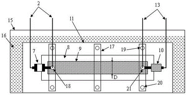
[0084] The test device for the nonlinear photoconductive switch to be tested includes a high-voltage pulse power supply, a Blumlein transmission line, a first high-voltage probe, a matching load, a plexiglass box, transformer insulating oil, and a limit fixture. The Blumlein transmission line includes a first glass-ceramic plate transmission line and a second glass-ceramic plate transmission line, the first glass-ceramic plate transmission line and the second glass-ceramic plate transmission line are superimposed on the plexiglass base, and the Blumlein transmission line is fixed on the plexiglass base by a limit fixture. On the plexiglass base; the silver electrode on one end of the first glass-ceramic flat transmission line is adjacent to and connected to the silver electrode on one end...


PUM


Abstract

The invention relates to the field of non-linear photoconductive semiconductor switch parameter testing, in particular to a non-linear photoconductive semiconductor switch testing device and method. The non-linear photoconductive semiconductor switch testing device and method are provided for solving the problems existing in the prior art. Through cooperation of a delay synchronous machine, a laser, an optical fiber, a photoelectric probe, a first high-voltage probe and the like, the difficulty of conducting accurate testing on a non-linear photoconductive semiconductor switch on the high-voltage, high-current and ultrafast-pulse conditions is overcome, and accurate, convenient and reliable testing of the parameters such as the conduction delay time, jittering, the conduction resistance, the withstand voltage and the service life of the non-linear photoconductive semiconductor switch is realized. The device comprises the delay synchronous machine, the laser, the optical fiber, the photoelectric probe, high-voltage probes, an oscilloscope, a high-voltage pulse power source, Blumlein transmission wires, a matching load, an organic glass box, transformer insulating oil and limiting fixtures. The non-linear photoconductive semiconductor switch to be tested, the Blumlein transmission wires and the matching load are placed in the organic glass box and are immersed in the transformer insulating oil.

Description

technical field [0001] The invention relates to the field of testing parameters of a nonlinear photoconductive switch, in particular to a testing device and method for a nonlinear photoconductive switch. Background technique [0002] Photoconductive Semiconductor Switches (PCSS) are a new type of solid state switches that use pulsed lasers to excite photoconductive semiconductors to achieve impedance state switching. Since Jayaraman and Lee of the University of Maryland first discovered in 1972 that the response time of semiconductor materials to picosecond light pulses can be in the range of picoseconds, the research on the characteristics of photoconductive switches has attracted great attention of scientists from all over the world. Because the photoconductive switch has the advantages of fast conduction speed, high synchronization accuracy, and small trigger jitter, it has good application prospects in many fields such as medical dielectric wall accelerators, high-power ...

Claims


Application Information

Patent Timeline
IPC IPC(8): G01R31/327G01R31/12
Inventor 王卫夏连胜谌怡刘毅张篁
Owner INST OF FLUID PHYSICS CHINA ACAD OF ENG PHYSICS
Why Eureka
Try Eureka