Signal processing circuit, resolver digital converter, and multipath nested mirror amplifier
A technology of signal processing circuit and differential amplifier, applied in amplifiers, differential amplifiers, amplifiers using switched capacitors, etc., can solve problems such as difficulty in ensuring the amplification of input signals and comparison accuracy.
- Summary
- Abstract
- Description
- Claims
- Application Information
AI Technical Summary
Problems solved by technology
Method used
Image
Examples
no. 1 example
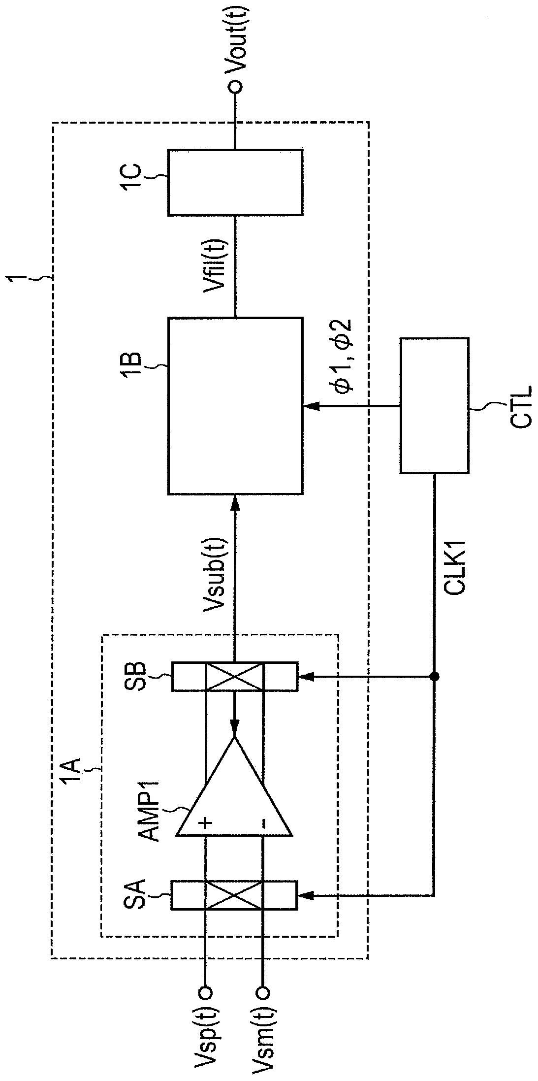
[0038] figure 1 A block diagram of the signal processing circuit 1 according to the first embodiment is shown.
[0039] The signal processing circuit 1 has a chopper amplifier 1A, an adder circuit 1B, and an output stage amplifier 1C. The chopper amplifier 1A has a modulation chopper circuit SA, a first-stage amplifier AMP1 and a demodulation chopper circuit SB. In the modulation chopper circuit SA and the demodulation chopper circuit SB, their chopping operations are controlled by the chopping clock CLK1 output from the control circuit CTL. In the adder circuit 1B, its operation is controlled by the control clock Φ1 and the control clock Φ2 output from the control clock circuit CTL.
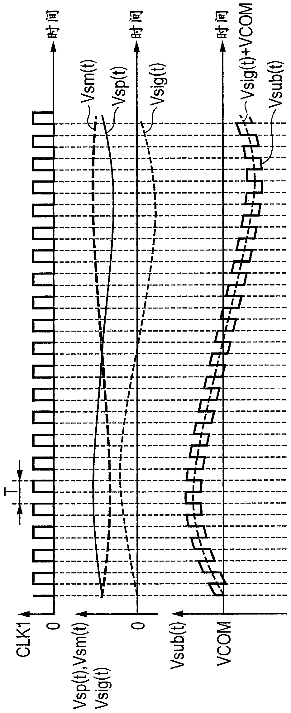
[0040] The differential input signal Vsp(t) and the differential input signal Vsm(t) are input into the modulation chopper circuit SA. Upon inverting the logic level of the chopping clock CLK1, the modulating chopper circuit SA is interchanging the differential input signal Vsp(t) applied to...
no. 2 example
[0138] Figure 10 A block diagram of a signal processing circuit 2 according to the second embodiment is shown.
[0139] exist Figure 10 in, is given with figure 1 Parts with the same sign as the sign have the same sign as figure 1 The configuration of the same configuration, and the description of each of these configurations is omitted.
[0140] The signal processing circuit 2 is equivalent to the following configuration so that the adder circuit 2B is replaced by figure 1 The adder circuit in 1B.
[0141] The signal processing circuit 2 has a chopper amplifier 1A, an adder circuit 2B, and an output stage amplifier 1C. The chopper amplifier 1A has a modulation chopper circuit SA, a first-stage amplifier AMP1 and a demodulation chopper circuit SB. In the modulation chopper circuit SA and the demodulation chopper circuit SB, their chopping operations are controlled by the chopping clock CLK1 output from the control circuit CTL. In the adder circuit 2B, its operation...
no. 3 example
[0170] Figure 14 A block diagram of a signal processing circuit 3 according to the third embodiment is shown.
[0171] exist Figure 14 in, is given with figure 1 Parts with the same sign as the sign have the same sign as figure 1 The configuration of the same configuration, and the description of each of these configurations is omitted. That is, the signal processing circuit 3 has a configuration in which in figure 1 In the signal processing circuit 1 shown in , the chopper amplifier 1A is replaced by a chopper amplifier 3A.
[0172] The signal processing circuit 3 has a chopper amplifier 3A, an adder circuit 1B, and an output stage amplifier 1C. The chopper amplifier 3A has a modulation chopper circuit SA and a configuration in which a two-stage single-ended amplifier and a demodulation chopper circuit SB are combined. In the modulation chopper circuit SA and the demodulation chopper circuit SB, their chopping operations are controlled by the chopping clock CLK1 ou...
PUM
 Abstract
Description
Claims
Application Information
 - R&D
- Intellectual Property
- Life Sciences
- Materials
- Tech Scout
- Unparalleled Data Quality
- Higher Quality Content
- 60% Fewer Hallucinations
Browse by: Latest US Patents, China's latest patents, Technical Efficacy Thesaurus, Application Domain, Technology Topic, Popular Technical Reports.
© 2025 PatSnap. All rights reserved.Legal|Privacy policy|Modern Slavery Act Transparency Statement|Sitemap|About US| Contact US: help@patsnap.com


