Coreless substrate processing method

A processing method and technology for coreless substrates, which are applied to the formation of electrical connection of printed components and the manufacture of multi-layer circuits, which can solve the problems of different board sizes, waste of pin board space, and difficult operation.

Active Publication Date: 2014-11-26
SHENNAN CIRCUITS
View PDF2 Cites 8 Cited by
  • Summary
  • Abstract
  • Description
  • Claims
  • Application Information

AI Technical Summary

Problems solved by technology

[0007] The inventors of the present invention have found through research and practice that the single-side build-up method only builds up the substrate on the same side of the support layer, so that the plate is prone to warping and the production speed is relatively slow; the double-side build-up method is to support The t

Method used


Image

  • Coreless substrate processing method
  • Coreless substrate processing method
  • Coreless substrate processing method

Examples


Embodiment Construction

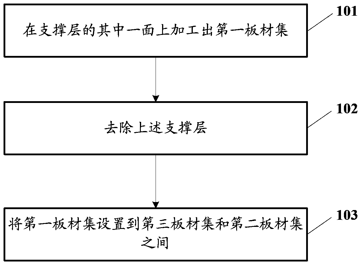
[0078] Embodiments of the present invention provide a processing method and processing equipment for a coreless substrate, in order to improve the production efficiency and yield of products.

[0079] In order to enable those skilled in the art to better understand the solutions of the present invention, the following will clearly and completely describe the technical solutions in the embodiments of the present invention in conjunction with the drawings in the embodiments of the present invention. Obviously, the described embodiments are only It is an embodiment of a part of the present invention, but not all embodiments. Based on the embodiments of the present invention, all other embodiments obtained by persons of ordinary skill in the art without making creative efforts shall fall within the protection scope of the present invention.

[0080] Each will be described in detail below.

[0081] The terms "first", "second", "third", "fourth", etc. (if any) in the description an...


PUM


Abstract

An embodiment of the invention discloses a coreless substrate processing method which comprises the following steps: carrying out processing to form a first board set on one surface of a support layer; removing the support layer; and arranging the first board set between a third board set and a second board set. The technical scheme provided in the embodiment of the invention helps to improve production efficiency and qualified rate of the products.

Description

technical field [0001] The invention relates to the field of circuit board processing and manufacturing, in particular to a processing method for a coreless substrate. Background technique [0002] Flip-chip packaging technology has been widely used in the packaging of high-frequency, high-speed and high-performance devices. The corresponding flip-chip packaging substrate also requires high pin count, high wiring density, high heat dissipation and good electrical performance. However, with the rapid development of network systems, terminal servers, and mobile communication devices, there are more and more requirements for high pin count, high-density wiring and high-speed packaging, which is specifically reflected in the fact that high pin count can achieve good impedance control , Low signal crosstalk, small signal attenuation and small parasitic effects. One of the main ways to achieve the above goals is to improve the substrate manufacturing technology. Its specific perf...

Claims


Application Information

Patent Timeline
IPC IPC(8): H05K3/46H05K3/40
Inventor 鲍平华丁鲲鹏姚腾飞
Owner SHENNAN CIRCUITS
Why Eureka
Try Eureka