Integrated LED element with epitaxial structure and packaging substrate integrated and manufacturing method

An epitaxial structure, packaging substrate technology, applied in the direction of electrical components, semiconductor devices, electric solid devices, etc., to achieve high power density and reduced thermal resistance.

Active Publication Date: 2018-03-02
JADE BIRD DISPLAY SHANGHAI LTD
View PDF6 Cites 1 Cited by
  • Summary
  • Abstract
  • Description
  • Claims
  • Application Information

AI Technical Summary

Problems solved by technology

To meet the further requirements of LED lighting for high power density, high output luminous flux, high effective service life, and low manufacturing cost, Figure 1A as well as Figure 1B The prior art LED components have inherent developmental limitations

Method used


Image

  • Integrated LED element with epitaxial structure and packaging substrate integrated and manufacturing method
  • Integrated LED element with epitaxial structure and packaging substrate integrated and manufacturing method
  • Integrated LED element with epitaxial structure and packaging substrate integrated and manufacturing method

Examples


Embodiment Construction

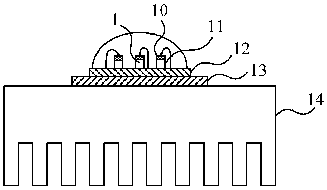
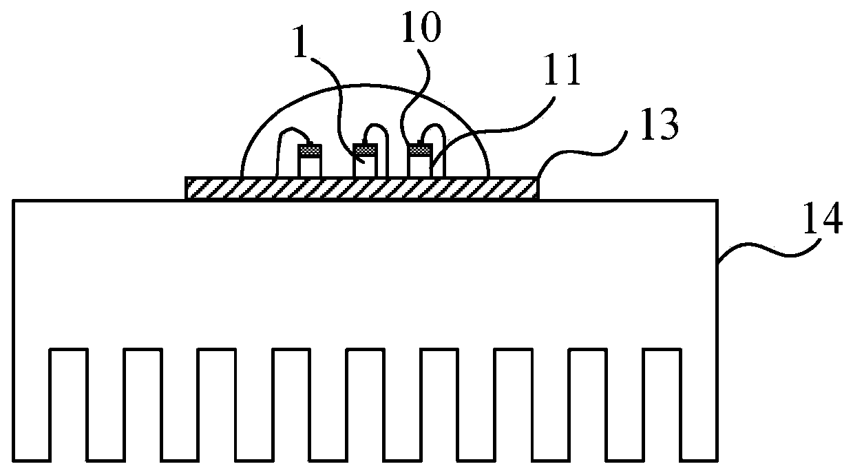
[0089] Therefore, an integrated LED element combined with an epitaxial structure and a packaging substrate of the present invention and its manufacturing method can effectively reduce the manufacturing process of LED elements, save materials, reduce costs, and effectively reduce the layer-by-layer heat conduction of LED elements. resistance, improve the characteristics of the LED element, and solve the problems of the prior art.

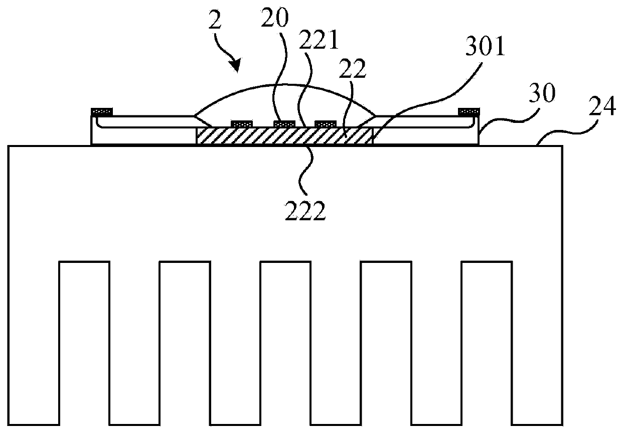
[0090] see Figure 2A and Figure 2B , Figure 2A as well as Figure 2B The structure schematic diagrams of the LED epitaxial structure, the LED package and its arrangement on the bare empty carrier and the LED heat dissipation and heat conduction elements shown in the integrated LED element of the present invention are respectively shown. According to a specific embodiment, the LED element 2 integrated with the epitaxial structure and the packaging substrate of the present invention can be embedded in a bare empty area 301 of a bare empty carrier...


PUM


Abstract

The invention discloses an integrated LED element with an epitaxial structure integrated with a packaging substrate and a manufacturing method. An LED element is formed by directly forming an LED epitaxial structure, electrodes, wires, etc. on a substrate to become an independent integrated LED element. . The LED element is a polycrystalline module structure, and can also be a single crystal structure. The LED element can be embedded in a bare empty carrier body, and through the support of the bare empty carrier body, the lower surface of the substrate of the LED element can be directly placed and contacted on a heat conduction or heat dissipation element. The LED element is directly fabricated on the wafer and cut into an independent element. The structure of the LED element can be a vertical structure or a horizontal structure according to different manufacturing methods.

Description

technical field [0001] The present invention relates to an integrated LED element that combines an epitaxial structure and a packaging substrate and a manufacturing method thereof, in particular, relates to directly using the carrying substrate carrying the LED epitaxial structure as a packaging substrate, and packaging the original LED grain The process completes the LED element on the substrate, so that the substrate can be directly placed and contacted with a heat conduction or heat dissipation element when the LED element is applied. The integrated LED element is manufactured directly on the wafer and then cut to become an independent element, and LED elements with a vertical structure or a horizontal structure can be produced according to different processes. Background technique [0002] For the LED lighting industry, the general product and industrial division of labor mode is to separate the production of LED grains and LED packaging into two completely independent p...

Claims


Application Information

Patent Timeline
Patent Type & Authority Patents(China)
IPC IPC(8): H01L25/075H01L33/48H01L33/64H01L33/62
CPCH01L2224/73267H01L2924/181H01L2224/19H01L2224/24137H01L2224/2518H01L2224/32225H01L2224/32245H01L2224/48091H01L2924/00014H01L2924/00012
Inventor 陈振贤
Owner JADE BIRD DISPLAY SHANGHAI LTD
Why Eureka
Try Eureka