A circuit board and a manufacturing method thereof

A circuit board manufacturing and circuit board technology, which is applied in the direction of printed circuit manufacturing, printed circuit, printed circuit components, etc., can solve the problems of unfavorable thinning of circuit board, increase of thickness of solder mask layer, unfavorable production of conductive lines, etc.

Inactive Publication Date: 2014-12-17
QI DING TECHNOLOGY QINHUANGDAO CO LTD +1
View PDF6 Cites 10 Cited by
  • Summary
  • Abstract
  • Description
  • Claims
  • Application Information

AI Technical Summary

Problems solved by technology

When the thickness of the wire circuit is large, the thickness of the formed solder resist layer also needs to be increased, which is not conducive to the thinning of the circuit board.
[0003] Moreover, the manufacturing method of the conductive circuit in the prior art is also unfavorable for the manufacture of the thin circuit.

Method used


Image

  • A circuit board and a manufacturing method thereof
  • A circuit board and a manufacturing method thereof
  • A circuit board and a manufacturing method thereof

Examples


Embodiment Construction

[0020] Hereinafter, specific embodiments are used to illustrate the circuit board manufacturing method provided by the technical solution.

[0021] The circuit board manufacturing method provided by the embodiment of the technical solution comprises the following steps:

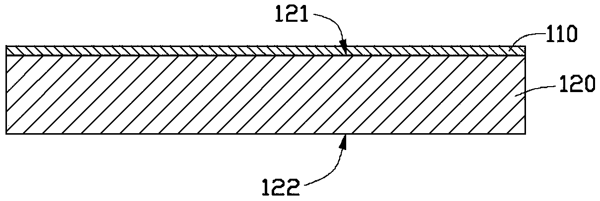
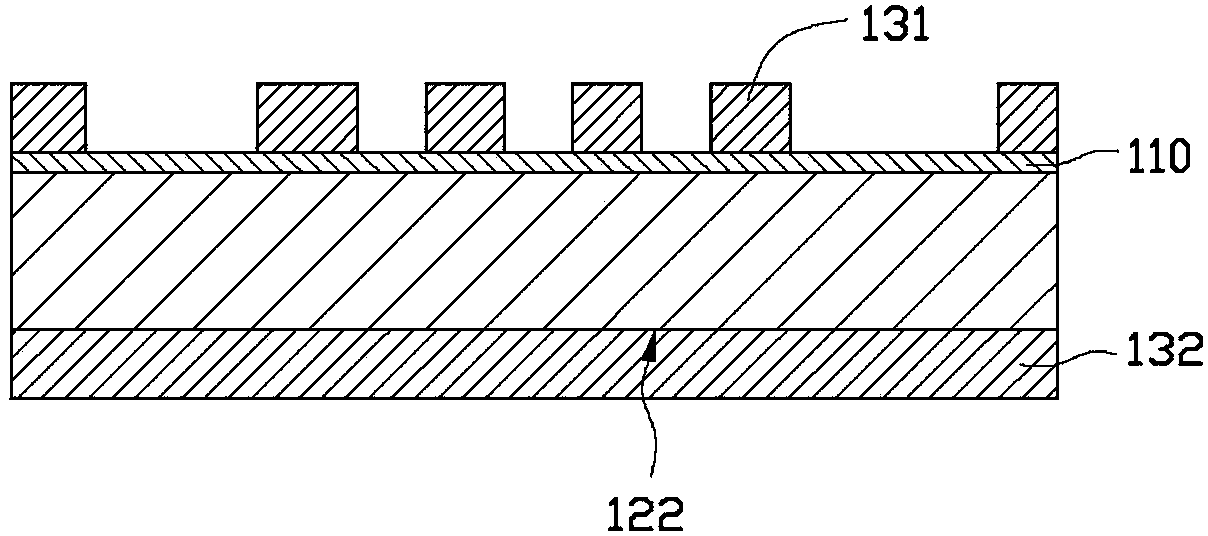
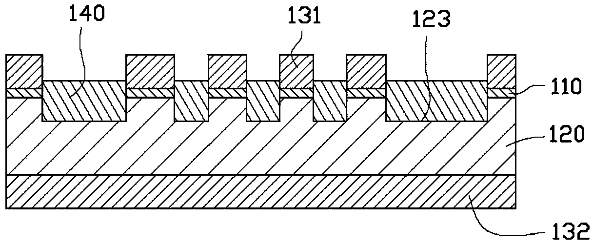
[0022] For a first step, see figure 1 , providing a first copper foil 110 and a metal carrier 120 .

[0023] The first copper foil 110 is a thin copper foil, and the thickness of the first copper foil 110 is 2 microns to 5 microns. The metal carrier 120 is made of a metal material different from that of the first copper foil 110 . In this embodiment, the metal carrier 120 is made of metal aluminum. It can be understood that the metal carrier 120 can also be made of other metals.

[0024] The thickness of the metal carrier 120 is greater than that of the first copper foil 110 , and the metal carrier 120 has sufficient mechanical strength to support the first copper foil 110 .

[0025] The metal carrier 12...


PUM


Abstract

The invention provides a circuit board, which comprises a dielectric layer, a first conductive circuit layer and a second conductive circuit layer. The first conductive circuit layer and the second conductive circuit layer are formed on the two opposite sides of the dielectric layer. The first conductive circuit layer is in part embedded in the dielectric layer, and in part protrudes from the dielectric layer, while the second conductive circuit layer is formed on the surface of the dielectric layer. The invention also provides a manufacturing method of the circuit board.

Description

technical field [0001] The invention relates to the technical field of circuit board production, in particular to a circuit board and a production method thereof. Background technique [0002] In the prior art, a build-up method or a semi-additive method is usually used in the manufacturing process of the circuit board, so that the obtained conductive lines are fabricated on the surface of the dielectric layer. That is, all the conductive lines protrude from the surface of the dielectric layer. In order to protect the conductive circuit, it is usually necessary to form a solder resist layer on the surface of the conductive circuit. The solder resist layer is usually formed by printing solder resist ink. When the solder resist layer is formed by printing, the solder resist layer needs to be formed to cover the conductive lines to be covered and the gaps between the conductive lines. Since the conductive circuit layer itself has a thickness, the thickness of the solder resis...

Claims


Application Information

Patent Timeline
Patent Type & Authority Applications(China)
IPC IPC(8): H05K1/02H05K3/06H05K3/18
Inventor 胡文宏
Owner QI DING TECHNOLOGY QINHUANGDAO CO LTD
Why Eureka
Try Eureka