Eureka AIR delivers breakthrough ideas for toughest innovation challenges, trusted by R&D personnel around the world.

Multipurpose wave absorbing film

A multi-purpose, film technology, applied in electrical components, magnetic field/electric field shielding, etc., can solve problems such as electromagnetic interference, human health hazards, abnormal work, etc., to achieve the effect of improving strength, improving utilization, and improving stability

Inactive Publication Date: 2014-12-17
斯迪克新型材料(江苏)有限公司
View PDF4 Cites 10 Cited by
  • Summary
  • Abstract
  • Description
  • Claims
  • Application Information

AI Technical Summary

Problems solved by technology

The electromagnetic waves released by electronic products will bring electromagnetic interference to other electronic devices around them, making them work abnormally; at the same time, they will also cause harm to human health

Method used


Image

  • Multipurpose wave absorbing film
  • Multipurpose wave absorbing film
  • Multipurpose wave absorbing film

Examples


Embodiment 1

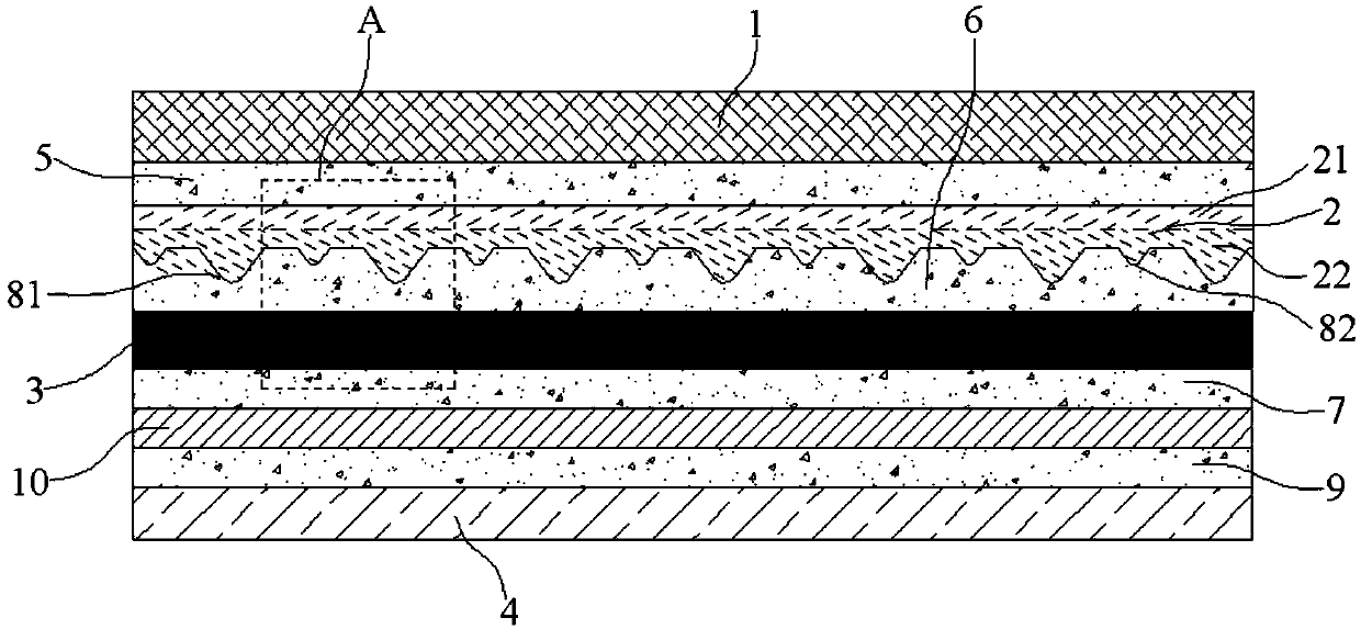
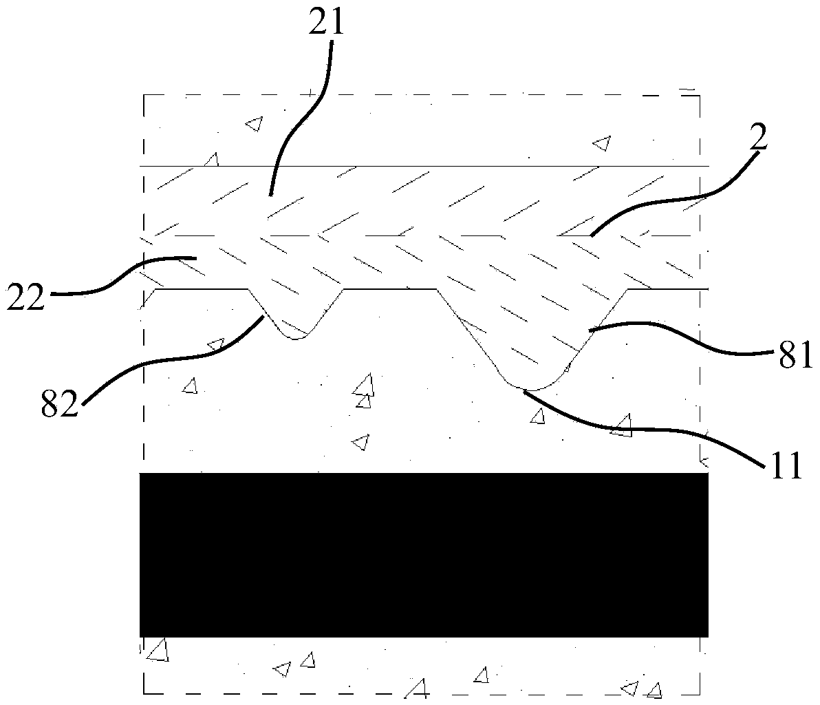
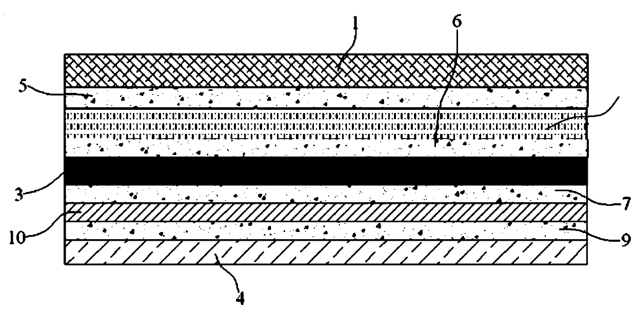
[0017] Example 1: A multi-purpose wave-absorbing film, including a PET insulating layer 1, a composite metal layer 2, a wave-absorbing layer 3, and a release material layer 4; a first glue is arranged between the PET insulating layer 1 and the composite metal layer 2 Adhesive layer 5, a second adhesive layer 6 is provided between the composite metal layer 2 and the wave-absorbing layer 3, the composite metal layer 2 is composed of a copper layer 21 and an aluminum foil layer 22, the composite metal layer 2 and The surface in contact with the absorbing layer 3 has several first prism protrusions 81 and first prism protrusions 82, the height of the first prism protrusions 81 is greater than the height of the second prism protrusions 82, the first The prism protrusions 81 and the second prism protrusions 82 are alternately arranged and there is a gap 9 between the respective bottoms of the adjacent first prism protrusions 81 and the second prism protrusions 82; the wave-absorbing ...

Embodiment 2

[0021] Example 2: A multi-purpose wave-absorbing film, including a PET insulating layer 1, a composite metal layer 2, a wave-absorbing layer 3, and a release material layer 4; a first glue is arranged between the PET insulating layer 1 and the composite metal layer 2 Adhesive layer 5, a second adhesive layer 6 is provided between the composite metal layer 2 and the wave-absorbing layer 3, the composite metal layer 2 is composed of a copper layer 21 and an aluminum foil layer 22, the composite metal layer 2 and The surface in contact with the absorbing layer 3 has several first prism protrusions 81 and first prism protrusions 82, the height of the first prism protrusions 81 is greater than the height of the second prism protrusions 82, the first The prism protrusions 81 and the second prism protrusions 82 are alternately arranged and there is a gap 9 between the respective bottoms of the adjacent first prism protrusions 81 and the second prism protrusions 82; the wave-absorbing ...


PUM

PropertyMeasurementUnit
heightaaaaaaaaaa
heightaaaaaaaaaa
heightaaaaaaaaaa

Abstract

The invention discloses a multipurpose wave absorbing film which comprises a PET insulation layer, a composite metal layer, a wave absorbing layer and a release material layer. A first adhesive layer is disposed between the PET insulation layer and the composite metal layer. A second adhesive layer is disposed between the composite metal layer and the wave absorbing layer. The composite metal layer is overlapped by a copper layer and an aluminum foil layer. The surface, contacting with the wave absorbing layer, of the composite metal layer is provided with a plurality of first prism protruding parts and second prism protruding parts, the first prism protruding parts are higher than the second prism protruding parts, and the first prism protruding parts and the second prism protruding parts are arranged alternately. A third adhesive layer, a polypropylene film layer and a fourth adhesive layer are sequentially disposed between the wave absorbing layer and the release material layer. The multipurpose wave absorbing film has the advantages that by the composite metal layer, multi-time absorbing can be formed, tape wave absorbing performance is increased evidently, heat dissipation is facilitated, film upwarp caused by temperature rise is avoided, and product performance stability is increased.

Description

technical field [0001] The invention belongs to the technical field of electronic materials, in particular to a multipurpose wave-absorbing film. Background technique [0002] The development of the electronics and communication industry is advancing by leaps and bounds, and more and more electronic and electrical products have entered the lives of ordinary people. While these products improve people's quality of life, they also bring about a prominent problem, that is, the problem of electromagnetic radiation. The electromagnetic waves released by electronic products will bring electromagnetic interference to other electronic devices around them, making them work abnormally; at the same time, they will also cause harm to human health. [0003] At present, miniaturization and high integration are the mainstream trends in the development of electronic products, and the internal space of these products is relatively small. Among the wave-absorbing materials, the chip-type wa...

Claims


Application Information

Patent Timeline
Patent Type & Authority Applications(China)
IPC IPC(8): H05K9/00
Inventor 金闯梁豪
Owner 斯迪克新型材料(江苏)有限公司
Why Eureka
Eureka Blog
Learn More