Semiconductor device and production method for semiconductor device

A semiconductor, conductive type technology, applied in semiconductor/solid-state device manufacturing, semiconductor devices, transistors, etc., can solve the problem of large reverse leakage current, improve the trade-off relationship, and reduce the effect of high temperature reverse leakage current

Inactive Publication Date: 2014-12-17
FUJI ELECTRIC CO LTD
View PDF8 Cites 11 Cited by
  • Summary
  • Abstract
  • Description
  • Claims
  • Application Information

AI Technical Summary

Problems solved by technology

[0018] However, the reverse blocking IGBT has the problem of large reverse leakage current when the gate is turned off and a reverse voltage is applied

Method used


Image

  • Semiconductor device and production method for semiconductor device
  • Semiconductor device and production method for semiconductor device
  • Semiconductor device and production method for semiconductor device

Examples


Embodiment approach

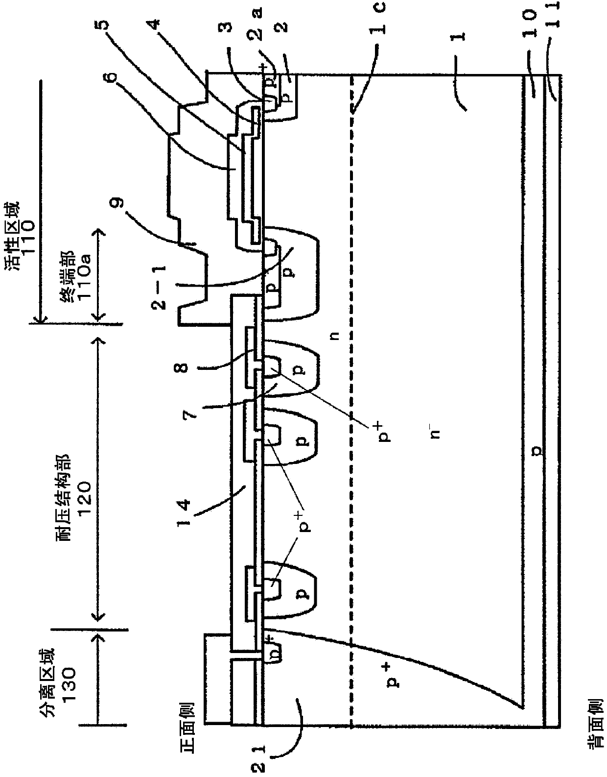
[0046] The reverse blocking type semiconductor device according to the embodiment of the present invention will be described taking a reverse blocking IGBT as an example. figure 1 It is a sectional view showing the structure of main parts of the reverse blocking IGBT according to the embodiment of the present invention. Such as figure 1 As shown, the reverse blocking IGBT according to the embodiment includes: an active region 110 disposed near the center of the chip, a voltage-resistant structure 120 disposed on the outer peripheral side surrounding the active region 110 , and a structure surrounding the voltage-resistant structure 120 . Outer separation zone 130 . Separation region 130 has p + type separation layer 21 as the main area, the p + type separation layer 21 is used to connect n - One main surface and the other main surface of the type semiconductor substrate. That is, p + The type separation layer 21 is set to penetrate n in the depth direction - type semi...


PUM


Abstract

The invention provides a semiconductor device and a production method for the semiconductor device. The depth of a terminal end p base region (2-1) provided in a terminal end section (110a) on the withstand voltage structure (120) side of an active region (110) is greater than the depth of a p-type base region (2) further on the inside than the terminal end p base region (2-1). An n-type high-density region (1c) is provided in the entire surface layer of one main surface of a semiconductor substrate, said region (1c) having a depth of no more than 20 [mu]m, from one main surface of the semiconductor substrate to the lower part of the floor section of the terminal end p base region (2-1). The ratio between the impurity concentration (n1) in the n-type high-density region (1c) and the impurity concentration (n2) in an n-type drift region (1) fulfills 1.0<n1 / n2<=5.0. As a result, the inverse leakage current when element operation temperatures are high can be reduced, the trade-off between the on voltage and switching loss can be improved, and overshoot peak voltages in collector voltages during turn off can be suppressed.

Description

technical field [0001] The present invention relates to a reverse blocking IGBT (reverse blocking IGBT) and a manufacturing method thereof which improve the trade-off relationship between the reverse leakage current of the reverse withstand voltage and the on-state voltage and the switching loss. Background technique [0002] High withstand voltage discrete power devices play a central role in power conversion devices. Such power devices include insulated gate bipolar transistors (IGBTs), or MOS gate (insulated gates made of metal-oxide-semiconductor) type field effect transistors (MOSFETs), and the like. Since the IGBT is a conductivity-modulated bipolar device, it has a lower on-state voltage than a unipolar device MOSFET. Therefore, IGBTs are often used in high withstand voltage devices for switching, in which on-state voltage tends to be high, and the like. [0003] Furthermore, when using a matrix converter with higher conversion efficiency as the above-mentioned powe...

Claims


Application Information

Patent Timeline
Patent Type & Authority Applications(China)
IPC IPC(8): H01L29/739H01L21/336H01L21/76H01L29/06H01L29/78
CPCH01L21/761H01L29/0646H01L29/1095H01L29/66333H01L29/7395H01L29/7397H01L29/42368H01L29/404H01L29/0834H01L29/0847H01L29/0619H01L21/2255H01L21/26513H01L29/36H01L21/225H01L21/265H01L29/66325H01L29/7393
Inventor 鲁鸿飞
Owner FUJI ELECTRIC CO LTD
Why Eureka
Try Eureka