Cleaning mechanism for silicon wafers

A technology for cleaning silicon wafers and cleaning tanks, applied in liquid cleaning methods, cleaning methods and utensils, chemical instruments and methods, etc., which can solve the problems of unrecoverable factory affairs, excessive acidity of waste lye, and reduction of the concentration of alkaline treatment liquid And other issues

Inactive Publication Date: 2014-12-24
MOTECH INDUSTRIES
View PDF5 Cites 7 Cited by
  • Summary
  • Abstract
  • Description
  • Claims
  • Application Information

AI Technical Summary

Problems solved by technology

As a result, the air knives, filters and liquid pipelines in the upstream and downstream cleaning tanks of the alkali tank 104 will be blocked, and the cleaning equipment will need to be shut down to clean the air knives, filters and pipelines
In addition, silicon wafers will be broken due to acid-base neutralized crystals on the transport device
Moreover, after the air knife

Method used


Image

  • Cleaning mechanism for silicon wafers
  • Cleaning mechanism for silicon wafers
  • Cleaning mechanism for silicon wafers

Examples


Embodiment Construction

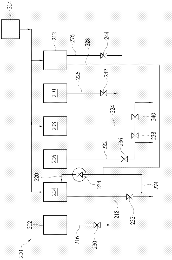
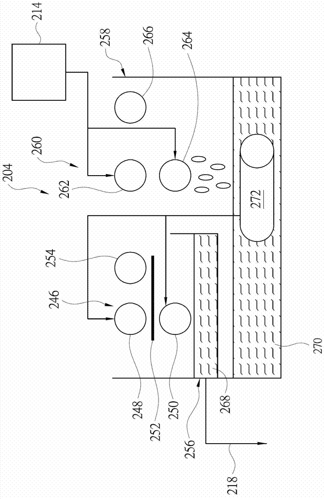
[0020] Please also refer to figure 2 and image 3 , figure 2 and image 3 It is a device schematic diagram of a silicon wafer cleaning mechanism according to an embodiment of the present invention, and a device schematic diagram of a cleaning station and two cleaning tanks of the silicon wafer cleaning mechanism. In this embodiment, the silicon wafer cleaning mechanism 200 mainly includes a first acid tank 202 , an alkali tank 206 , a cleaning station 204 , a drain valve 232 and a pump device 272 . In one embodiment, the first acid tank 202 may be filled with an acid solution such as hydrofluoric acid (HF) to perform wet processing such as etching on the silicon wafer 252 . In some examples, the silicon wafer cleaning mechanism 200 may be further provided with a pipeline 216 and a drain valve 230 according to process requirements, wherein the pipeline 216 communicates with the first acid tank 202 , and the drain valve 230 is disposed on the pipeline 216 . The discharge o...


PUM


Abstract

The invention provides a cleaning mechanism for silicon wafers. The cleaning mechanism for the silicon wafers comprises the components of: a first acid trough, an alkali trough, a first cleaning trough, a first flushing device, a water discharging valve, a second cleaning trough, a second flushing device and a pump device. The first flushing device is arranged between the first acid trough and the alkali trough. The first flushing device is arranged in the first cleaning trough. The first cleaning trough is suitable for receiving first cleaning liquid after cleaning by the first flushing device. The water discharging valve is communicated with the first cleaning trough. The first cleaning liquid is discharged through the water discharging valve. The second cleaning trough is arranged between the first cleaning trough and the alkali trough. The second flushing device is arranged in the second cleaning trough. The second cleaning trough is suitable for receiving second cleaning liquid after cleaning by the second flushing device. The pump device is suitable for circulating the second cleaning liquid to the first cleaning trough for use by the first flushing device.

Description

technical field [0001] The present invention relates to a cleaning mechanism, and in particular to a cleaning mechanism for silicon wafers. Background technique [0002] Please refer to figure 1 , figure 1 A device schematic diagram showing a traditional silicon wafer cleaning mechanism. The conventional silicon wafer cleaning mechanism 100 mainly includes a first acid tank 102 , a first cleaning tank 104 , an alkali tank 106 , a second cleaning tank 108 , a second acid tank 110 , a third cleaning tank 112 and a cleaning solution supply source 114 . From upstream to downstream of the process, a first acid tank 102 , a first cleaning tank 104 , an alkali tank 106 , a second cleaning tank 108 , a second acid tank 110 and a third cleaning tank 112 are arranged in sequence. [0003] The silicon wafer is first etched in the first acid bath 102 . After being etched by the acid solution, the silicon wafer is carried out of the first acid tank 102 and sent into the first cleanin...

Claims


Application Information

Patent Timeline
IPC IPC(8): B08B3/04B08B3/02B08B3/08
CPCB08B3/022B08B3/041B08B3/08
Inventor 陈豪忠许景勋
Owner MOTECH INDUSTRIES
Why Eureka
Try Eureka