Atomic layer deposition equipment

A technology of atomic layer deposition and equipment, which is applied in the direction of coating, metal material coating process, gaseous chemical plating, etc., can solve the problems of long time consumption, low production capacity of atomic layer deposition equipment, and reduced production capacity of atomic layer deposition equipment

Active Publication Date: 2014-12-24
BEIJING NAURA MICROELECTRONICS EQUIP CO LTD
View PDF3 Cites 165 Cited by
  • Summary
  • Abstract
  • Description
  • Claims
  • Application Information

AI Technical Summary

Problems solved by technology

[0007] First, the deposition rate of atomic layers is slow due to the self-inhibiting nature of the reaction between the gases from the two sources (i.e., the two cannot continue to react) and it takes a significant amount of time to complete all of the above process steps , For example, it takes at least 300-400s to deposit an aluminum oxide film with a thickness of 20nm, which makes the productivity of atomic layer deposition equipment very low, and it is difficult to meet the needs of large-scale production
[0008] Its two, before carrying out step 4, that is, before passing into the next gas in the reaction chamber 14, all need to carry out the step of removing the gas remaining in the reaction chamber 14 by means of the purge gas, which makes the whole process complete. A large portion of the process time is consumed in this step, which further reduces the throughput of the ALD tool

Method used


Image

  • Atomic layer deposition equipment
  • Atomic layer deposition equipment
  • Atomic layer deposition equipment

Examples


Embodiment Construction

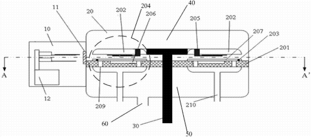
[0051] In order to enable those skilled in the art to better understand the technical solutions of the present invention, the atomic layer deposition equipment provided by the present invention will be described in detail below with reference to the accompanying drawings.

[0052] Figure 3A It is a cross-sectional view of the atomic layer deposition equipment provided by the first embodiment of the present invention. Figure 3B for Figure 3A A top view along the line A-A' in the center. Figure 3C for Figure 3A Top view of the middle and lower cover. Please also refer to Figure 3A , Figure 3B and Figure 3C , the atomic layer deposition apparatus includes a loading chamber 10 , a gate valve 11 and a reaction chamber 20 . Wherein, the reaction chamber 20 includes a plurality of sub-chambers and a driving unit 30, wherein four process positions 204 are arranged on the same horizontal plane (that is, a plane parallel to the upper surface of the substrate 201) in the rea...


PUM


Abstract

The invention provides atomic layer deposition equipment. The atomic layer deposition equipment comprises a reaction chamber which comprises a plurality of sub chambers and a drive unit, wherein a plurality of process positions are arranged on the same horizontal plane in the reaction chamber, the plurality of process positions are arranged at intervals along the peripheral direction of the reaction chamber, and are uniformly arranged in sequence according to the sequence of processes, the quantity and positions of the sub chambers are in one-to-one correspondence with those of the process positions, and each sub chamber is used for completing one process of single processes for a substrate in each sub chamber; the drive unit is used for enabling each substrate to complete the corresponding process in the sub chamber placed on the position of each process according to the sequence of the process. The automatic layer deposition equipment provided by the invention can be used for processing a plurality of substrates at the same time by a single process, so that the process efficiency is improved, and thus, the yield is increased.

Description

technical field [0001] The invention belongs to the technical field of microelectronic processing, and in particular relates to an atomic layer deposition device. Background technique [0002] In the field of microelectronics processing technology, atomic layer deposition (ALD) is a device that deposits substances layer by layer on the surface of a substrate in the form of a single atomic film. Due to the diversity of deposition materials and the accuracy of deposition thickness, it has been more and more widely used. [0003] ALD is a chemical vapor deposition (CVD) method based on ordered, surface self-saturated reactions. Different from other CVD film forming methods (such as PECVD), two or more gas sources (source A, source B, source C, etc.) In order to prevent the mutual influence between different sources, it is necessary to purge (Purge) with other gases (such as Ar) that do not participate in the reaction between the pulses of different sources. [0004] figure ...

Claims


Application Information

Patent Timeline
Patent Type & Authority Applications(China)
IPC IPC(8): C23C16/44C23C16/455C23C16/458
Inventor 南建辉宋巧丽李强王宝全苏晓峰
Owner BEIJING NAURA MICROELECTRONICS EQUIP CO LTD
Why Eureka
Try Eureka