Solar silicon wafer and battery piece counting method based on image processing

A solar silicon wafer and image processing technology, applied in the field of image processing, can solve the problems of not widely used, damaged, error-prone silicon wafers or battery chips, etc.

Active Publication Date: 2014-12-24
ZHENJIANG SYD TECH CO LTD
View PDF4 Cites 17 Cited by
  • Summary
  • Abstract
  • Description
  • Claims
  • Application Information

AI Technical Summary

Problems solved by technology

The thickness of solar silicon wafers and solar cells is very thin, generally around 180 microns, with a plus or minus error of 20 microns. There are various counting methods, including manual visual inspection, laser scanning inspection, infrared inspection and machine vision in

Method used


Image

  • Solar silicon wafer and battery piece counting method based on image processing
  • Solar silicon wafer and battery piece counting method based on image processing
  • Solar silicon wafer and battery piece counting method based on image processing

Examples


Embodiment Construction

[0063] The present invention will be further described below in conjunction with the accompanying drawings and specific embodiments.

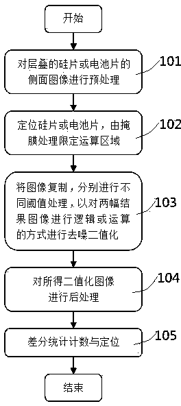
[0064] Such as figure 1 Shown, the method for counting solar silicon wafers and cells based on image processing comprises the following steps:

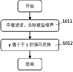
[0065] Step 101, preprocessing the side image of the stacked silicon wafer or battery sheet, such as figure 2 Shown:

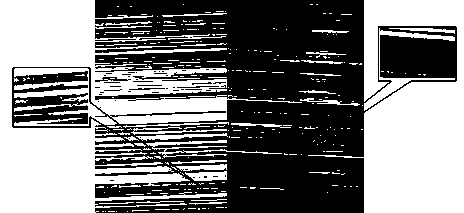
[0066] Step 1011, perform median filtering on the side image of the laminated silicon wafer or cell to remove the salt and pepper noise, such as image 3 As shown, among them, image 3 The picture in part a is the side image of the silicon wafer, and the picture in part b is the side image of the solar cell; due to the uneven illumination and the inherent characteristics of the side of the silicon wafer and the cell, it often appears on the obtained side image of the stacked silicon wafer or cell. The salt-and-pepper noise superimposed on the image in the form of black and white d...


PUM


Abstract

The invention discloses a solar silicon wafer and battery piece counting method based on image processing and belongs to the technical field of image processing. The method comprises the following steps that 101, side images of stacked silicon wafers or stacked battery pieces are preprocessed; 102, a measured object is positioned, and a mask is used for processing and limiting an operation region; 103, the images covered with the mask are replicated and subjected to different kinds of threshold processing respectively to obtain a denoised and binarized image; 104, the obtained denoised and binarized image is subjected to post-processing; 105, differential statistical counting and positioning are conducted to obtain the number of the measured stacked silicon wafers or the measured stacked battery pieces. According to the method, the side images of the stacked silicon wafers or the stacked battery pieces are collected, the binary image highlights gaps and filters out other interference noise, and finally a differential statistical algorithm is adopted to obtain the accurate number. By means of the method, the problem of inaccurate counting due to poor quality of the obtained image and high noise is solved, and the counting accuracy and efficiency are improved.

Description

technical field [0001] The invention belongs to the technical field of image processing, and in particular relates to a method for counting solar silicon chips and battery chips based on image processing. Background technique [0002] During the production of solar wafers and cells, it is often necessary to count them. The thickness of solar silicon wafers and solar cells is very thin, generally around 180 microns, with a plus or minus error of 20 microns. There are various counting methods, including manual visual inspection, laser scanning inspection, infrared inspection and machine vision inspection. Manual visual inspection is error-prone and easily causes damage to silicon wafers or cells. Laser inspection and infrared inspection are costly, have low counting accuracy, and are easily restricted by the environment. These inspection technologies are not widely used. Due to the characteristics of non-contact, fast speed, high precision and rich lighting schemes, machine v...

Claims


Application Information

Patent Timeline
IPC IPC(8): G06T5/00
Inventor 孙智权张千童钢
Owner ZHENJIANG SYD TECH CO LTD
Why Eureka
Try Eureka