
Array type chip resistor and method of manufacturing thereof

A resistor, chip technology, applied in the direction of resistor manufacturing, resistors, thick film resistors, etc., can solve the problem of undisclosed adjacent side electrodes

Active Publication Date: 2014-12-24
SAMSUNG ELECTRO MECHANICS CO LTD
View PDF5 Cites 1 Cited by
  • Summary
  • Abstract
  • Description
  • Claims
  • Application Information

AI Technical Summary

Problems solved by technology

However, the above-mentioned patent documents do not disclose the relationship between the interval between adjacent side electrodes and their heights

Method used


Image

  • Array type chip resistor and method of manufacturing thereof
  • Array type chip resistor and method of manufacturing thereof
  • Array type chip resistor and method of manufacturing thereof

Examples


Embodiment Construction

[0049] Hereinafter, embodiments of the present invention will be described in detail with reference to the accompanying drawings. However, the present invention may be embodied in many different forms and should not be limited to the embodiments set forth herein. Rather, these embodiments are provided so that this disclosure will be thorough and complete, and will fully convey the scope of the invention to those skilled in the art. In the drawings, the shapes and dimensions of elements may be exaggerated for clarity, and the same reference numerals will be used throughout to designate the same or like elements.

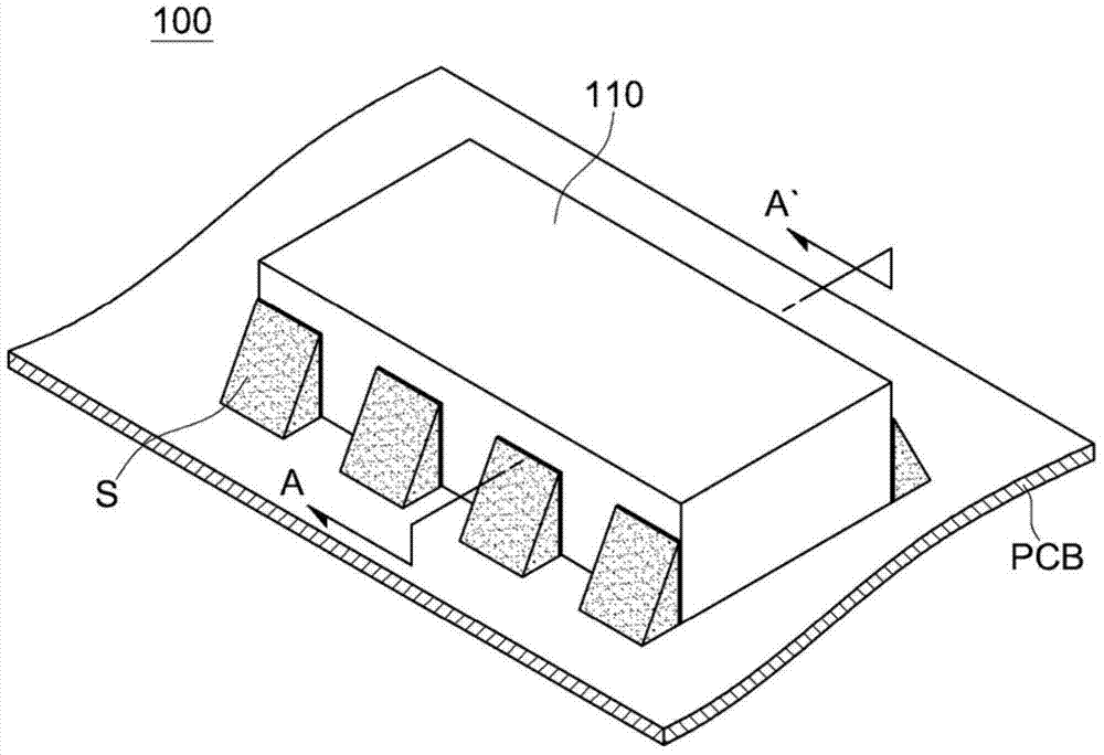
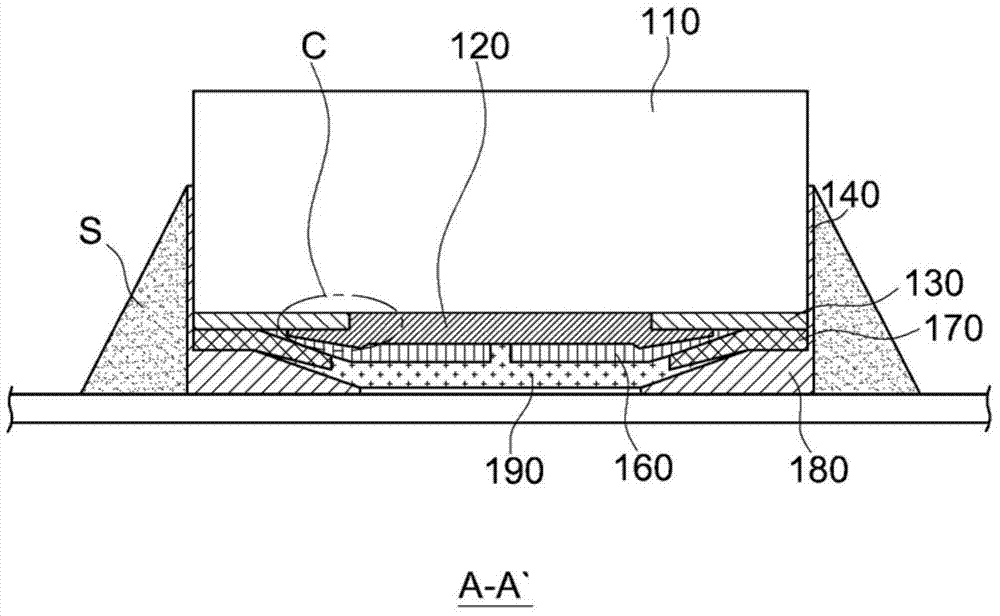
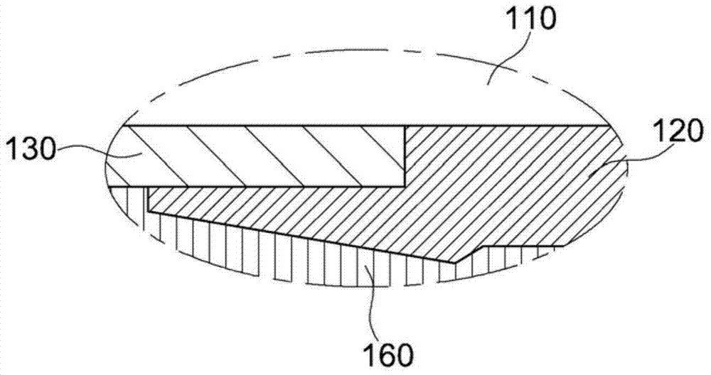
[0050] figure 1 is a schematic perspective view of an array type chip resistor according to an embodiment of the present invention, and figure 2 is along figure 1 A schematic cross-sectional view of the line A-A' of the array type chip resistor.

[0051] The array type chip resistor according to the embodiment of the present invention will be referred to figure ...


PUM


Abstract

There is provided an array type chip resistor including: a chip body, four pairs of lower electrodes disposed on both sides of a lower surface of the chip body and formed so as to be extended to edges of the chip body, side electrodes formed so that the lower electrodes are extended to sides of the chip body, and a resistor interposed between the lower electrodes on the lower surface of the chip body and electrically connected to the lower electrode through a contact portion, wherein when a width of the side electrode is defined as d1, a distance between adjacent side electrodes is defined as d2, and a height of the side electrode is defined as h, in the case in which d1 / d2 is 0.5 to 1.5, a value of h is 4,300 / d1 [mu]m or above and is 0.24d2+87.26 [mu]m or less.

Description

[0001] Cross References to Related Applications [0002] This application claims priority from Korean Patent Application No. 10-2013-0064483 filed with the Korean Intellectual Property Office on Jun. 5, 2013, the disclosure of which is hereby incorporated by reference. technical field [0003] The present invention relates to an array type chip resistor and a manufacturing method thereof, and more particularly, to an array type chip resistor capable of securing bonding strength and having improved reliability and a manufacturing method thereof . Background technique [0004] Demands for array-type chip resistors suitable for realizing precision resistors and thus being used in various electronic devices such as camcorders, digital cameras, and motor vehicles have been expanding. [0005] Generally, a memory module resistor in the form of an array type chip resistor is mounted near an external connection terminal of a module substrate. [0006] Array chip resistors are used...

Claims


Application Information

Patent Timeline
Patent Type & Authority Applications(China)
IPC IPC(8): H01C13/02H01C17/075H10N97/00
CPCH01C1/142H01L28/24H01C1/01H01C1/14H01C7/003H01C17/281H01C17/02H01C7/00H01L28/20
Inventor 金正逸黄夏星金海仁田中一郎权五星
Owner SAMSUNG ELECTRO MECHANICS CO LTD
Learn More