Packaging method for organic light-emitting diode display

An encapsulation method and electroluminescence technology, which can be applied to electric solid devices, circuits, electrical components, etc., can solve problems such as damage to organic functional layers, and achieve the effects of extending service life, strengthening mechanical strength, and fast packaging.

Inactive Publication Date: 2010-10-20
TRULY SEMICON
View PDF0 Cites 18 Cited by
  • Summary
  • Abstract
  • Description
  • Claims
  • Application Information

AI Technical Summary

Problems solved by technology

[0005] But even with the back cover and desiccant, there will still be a considerable amoun

Method used


Image

  • Packaging method for organic light-emitting diode display
  • Packaging method for organic light-emitting diode display
  • Packaging method for organic light-emitting diode display

Examples


Embodiment 1

[0033] This embodiment first introduces the structure of the OLED of the present invention.

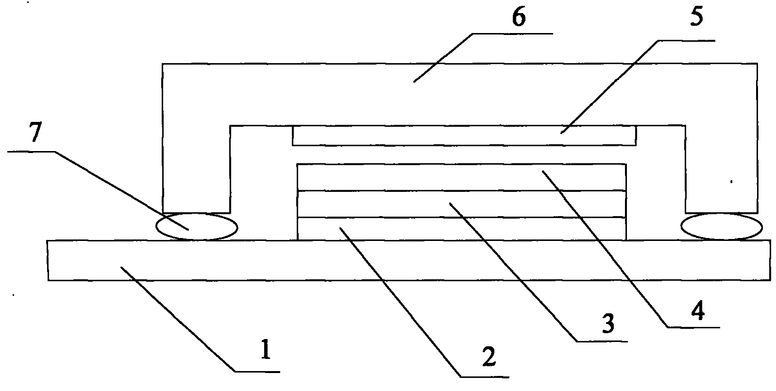
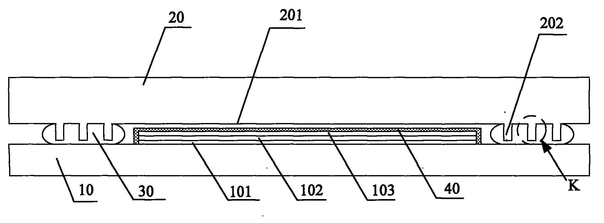
[0034] figure 2 is a schematic cross-sectional view of the OLED of the present invention. The invention provides an OLED, such as figure 2 As shown, the OLED includes: a substrate 10 , a back cover 20 , and an encapsulant 30 .

[0035] A pixel display area matrix is ​​formed on the substrate 10; each pixel display area in the pixel display area matrix includes a transparent anode 101, an organic functional layer 102 and a cathode 103 deposited on the substrate 10 in sequence. The surface of each pixel display area is covered with a water-absorbing protective layer 40; if the special conductive glass is selected for use in the preparation of the substrate 10, the pre-deposited ITO (Indium Tin Oxide, indium tin oxide) coating on the conductive glass can be used as The anode of the OLED is used.

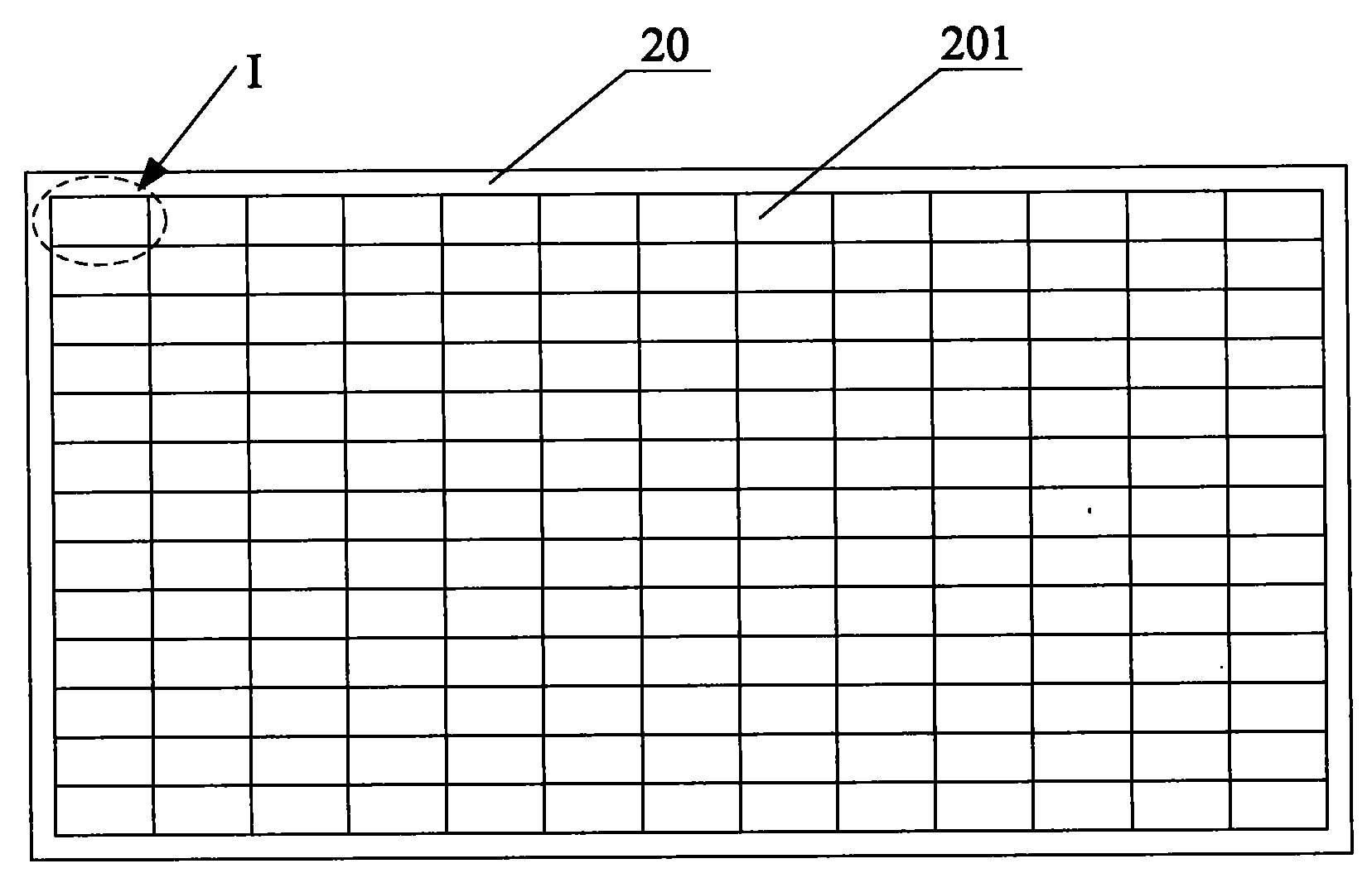
[0036] See also image 3 , Figure 4 ,in, image 3 It is a schematic bottom view o...

Embodiment 2

[0052] This embodiment introduces the encapsulation method of the above-mentioned OLED. The side of the rear cover of the OLED facing the substrate is formed with a light-emitting area corresponding to the pixel display area matrix on the substrate, and the back cover further includes at least one circle of continuous protrusions surrounding the light-emitting area on the periphery of the light-emitting area ; The surface of each pixel display area of ​​the substrate is covered with a water-absorbing protective layer. Such as Figure 9 As shown, the packaging method includes:

[0053] S10, coating encapsulation glue on the periphery of the light-emitting area of ​​the rear cover; the encapsulation glue surrounds the light-emitting area and completely covers at least one ring of protrusions surrounding the light-emitting area.

[0054] The height of the protrusions may be 5-100 μm, and the width may be 5-200 μm. The material of the water-absorbing protective layer may be an ...


PUM

PropertyMeasurementUnit
Heightaaaaaaaaaa
Widthaaaaaaaaaa
Thicknessaaaaaaaaaa

Abstract

The invention discloses a packaging method for an organic light-emitting diode (OLED) display. A rear cover of the organic light-emitting diode display also comprises at least one ring of continuous bumps surrounding the light emitting region at the periphery of the light emitting region; and a water-absorbing protection layer covers the surface of each pixel display region of a substrate. The method comprises the following steps of: coating a packaging adhesive at the periphery of the light emitting region of the rear cover, wherein the packaging adhesive surrounds the light emitting region and completely covers the at least one ring of bumps surrounding the light emitting region; aligning and pressing the rear cover coated with the packaging adhesive and the substrate; and curing the packaging adhesive. By using the rear cover provided with bumps at the periphery of the light emitting region, the required adhesive strength between the rear cover and the substrate can be ensured, the distance between the rear cover and the substrate can be greatly reduced, and the capability of the OLED of preventing the penetration of vapor and oxygen can be enhanced; and the vapor penetrated into the OLED can be adsorbed by further covering a transparent water-absorbing protection layer on the pixel display region, so that the organic functional layer is protected.

Description

technical field [0001] The invention relates to the technical field of electronic appliances, in particular to a packaging method for an organic electroluminescence display. Background technique [0002] Organic light-emitting display (OLED, Organic Light-Emitting Diode) is an emerging flat-panel display at present, because OLED has active light emission, high contrast, can be thinned, fast response, no viewing angle limit, wide operating temperature range, low With many advantages such as power consumption, strong shock resistance and flexible display, it is recognized as the main force of the next generation of displays. [0003] The typical structure of the existing OLED is as figure 1 As shown, it includes: a substrate glass 1, an anode 2 deposited on the substrate glass 1, an organic functional layer 3 covering the anode 2, a cathode 4 located on the organic functional layer 3, a back cover 6 corresponding to the substrate glass 1, The desiccant 5 attached to the ligh...

Claims


Application Information

Patent Timeline
IPC IPC(8): H01L51/56H01L51/50H01L51/52
Inventor 曹绪文刘然何基强
Owner TRULY SEMICON
Why Eureka
Try Eureka