Component embedded package structure and its manufacturing method
A packaging structure, embedded technology, used in semiconductor/solid state device manufacturing, electrical components, semiconductor devices, etc.
- Summary
- Abstract
- Description
- Claims
- Application Information
AI Technical Summary
Problems solved by technology
Method used
Image

Examples
Embodiment Construction
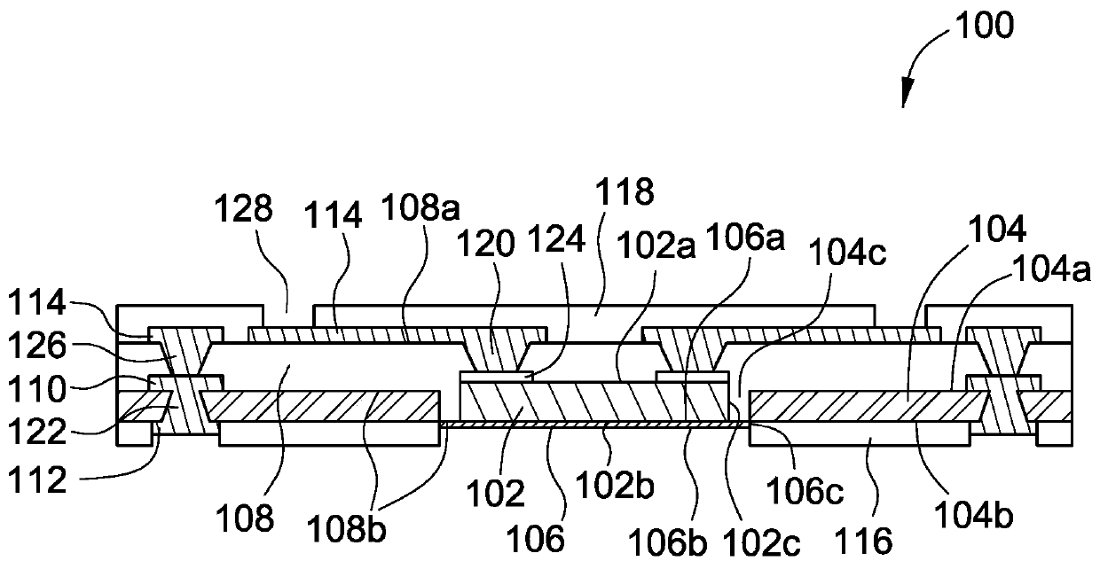
[0018] Please refer to figure 1 , which shows a cross-sectional view of an embodiment of a device-embedded packaging structure according to the present invention. The component embedded package structure 100 includes a bare chip 102, a substrate 104, a metal layer 106, a first dielectric layer 108, a first patterned conductive layer 110, a second patterned conductive layer 112, a third patterned conductive layer 114 and solder mask 116.
[0019] The die 102 has an active face 102a, a back face 102b opposite to the active face 102a, and a side face 102c. The backside 102 b of the die 102 is in direct contact with the metal layer 106 .
[0020] The substrate 104 has a first surface 104a and a second surface 104b opposite to the first surface 104a. In an embodiment, the substrate 104 has at least one first via 104c extending from the first surface 104a to the second surface 104b for receiving at least one die. The width and shape of the first through holes 104c are designed a...
PUM
 Abstract
Description
Claims
Application Information
 - R&D
- Intellectual Property
- Life Sciences
- Materials
- Tech Scout
- Unparalleled Data Quality
- Higher Quality Content
- 60% Fewer Hallucinations
Browse by: Latest US Patents, China's latest patents, Technical Efficacy Thesaurus, Application Domain, Technology Topic, Popular Technical Reports.
© 2025 PatSnap. All rights reserved.Legal|Privacy policy|Modern Slavery Act Transparency Statement|Sitemap|About US| Contact US: help@patsnap.com