Manufacturing method for thin coreless substrate

A technology of thin substrates and manufacturing methods, which is applied in the direction of multilayer circuit manufacturing, semiconductor/solid-state device manufacturing, and electrical connection formation of printed components, etc. It can solve the problems of increasing the difficulty of controlling the thickness of the line and the difficulty of arbitrary interconnection of circuits, etc., and achieves low cost. , reduce thickness and reduce cost

Active Publication Date: 2014-12-24
NAT CENT FOR ADVANCED PACKAGING
View PDF3 Cites 24 Cited by
  • Summary
  • Abstract
  • Description
  • Claims
  • Application Information

AI Technical Summary

Problems solved by technology

If the circuit pattern is made first, it is necessary to back-drill or make through holes, and then perform electroplating, which is not easy to realize arbitrary interconnection of the circuit, and increases the difficulty of controlling the thickness of the circuit

Method used


Image

  • Manufacturing method for thin coreless substrate
  • Manufacturing method for thin coreless substrate
  • Manufacturing method for thin coreless substrate

Examples


Embodiment 1

[0042] The manufacturing method of the coreless thin substrate of this embodiment includes the following steps:

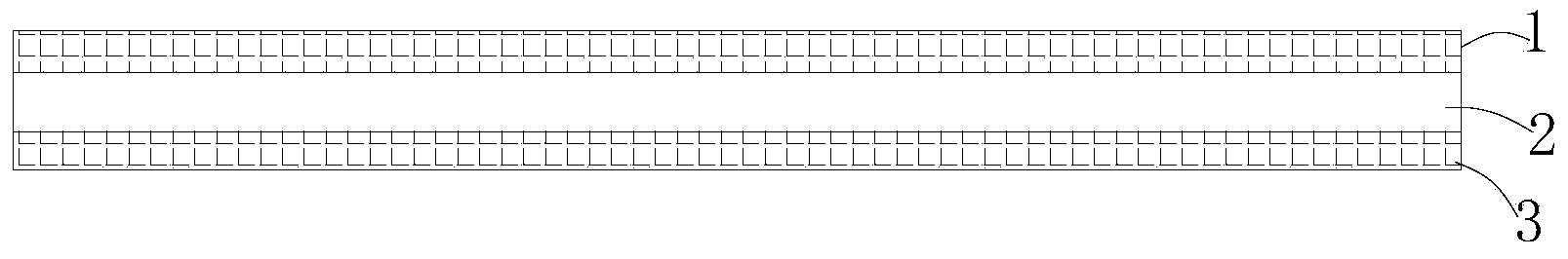
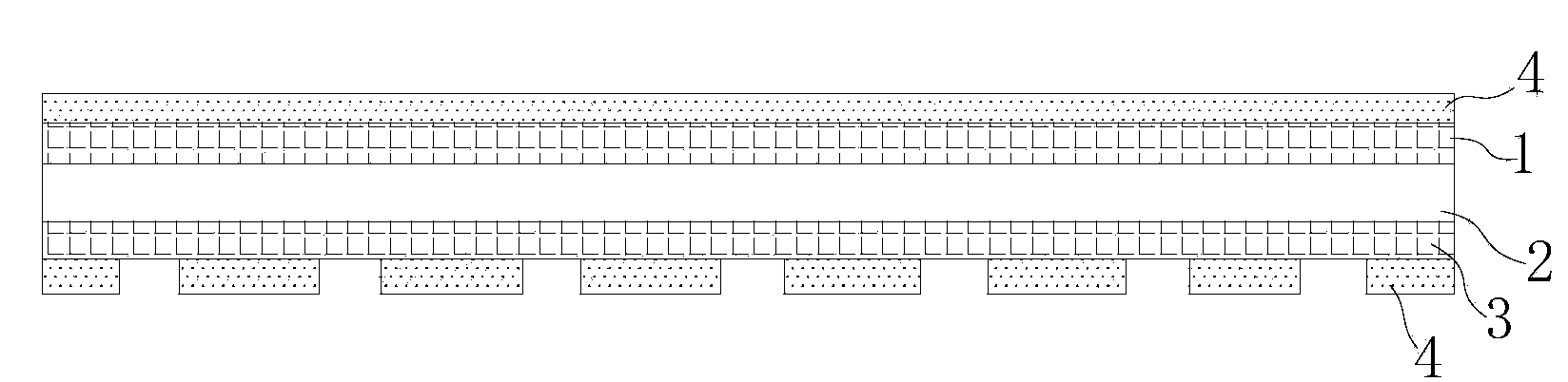
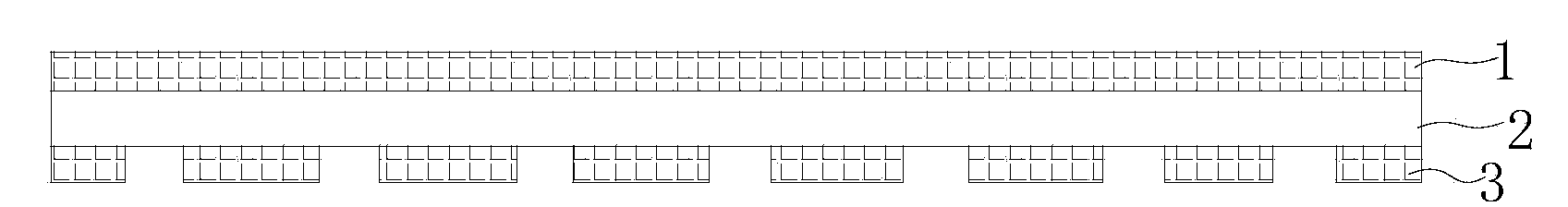
[0043] a. Laminate the first copper foil 1, the first prepreg 2, and the second copper foil 3 from top to bottom in order for the first pressing. The first pressing is low-temperature vacuum pressing, and the pressing temperature is the first prepreg The temperature at which the viscosity of 2 is the lowest, this embodiment is preferably 110°C, and it is pressed under a certain pressure with a vacuum laminator for 15-25 minutes, and it is preferably 20 minutes in this embodiment to obtain the first substrate, such as figure 1 As shown, the double-sided copper clad prepreg; the first substrate is subjected to dry film pretreatment, such as cleaning or acid treatment, and then the first dry film 4 is pressed on the surface of the first copper foil 1 and the second copper foil 3 respectively, and The first dry film 4 pressed on the surface of the second copper foil 3 is s...

Embodiment 2

[0050] This embodiment differs from embodiment 1 in that: after step d, step e2 replaces step e1, and the third prepreg 14 is laminated on both sides of the substrate model prepared in step d, and the third prepreg 14 is laminated on the third prepreg 14. Laminate a specific number of multi-layer circuits 15 to prepare a multi-layer odd-numbered board, such as Figure 15 As shown, the multilayer circuit is also respectively connected to the first circuit and the third circuit through blind holes. The build-up method used in this embodiment is just a conventional method for manufacturing a multilayer board, and will not be repeated here.


PUM


Abstract

The invention discloses a manufacturing method for a thin coreless substrate. The method comprises the steps of a, sequentially stacking first copper foil, first prepreg and second copper foil for conducting pressing fit for the first time to obtain a first substrate, and manufacturing a second circuit on the second copper foil, wherein the second circuit comprises a first bonding pad, and the first bonding pad extends towards the periphery to form an electroplating frame; b, on the premise that the electroplating frame is exposed, sequentially stacking second prepreg and third copper foil on the second copper foil for conducting pressing fit for the second time to obtain a second substrate, and manufacturing a first circuit and a third circuit respectively so as to obtain a substrate workblank; c, conducting pressing fit for the third time; d, forming a first blind hole and a second blind hole, and filling the first blind hole and the second blind hole by the adoption of the electroplating hole filling technology respectively to obtain a substrate model. The thin coreless substrate is manufactured through the manufacturing method, is a three-layer coreless substrate, has the symmetric pressing-fit condition and the pressing-fit structure, and achieves internal layer circuit embedment.

Description

Technical field [0001] The invention relates to the field of substrate processing, in particular to a method for manufacturing a substrate, and in particular to a method for manufacturing a coreless thin substrate. Background technique [0002] Coreless substrates (ie coreless substrates) are currently the hotspot of high-end substrate research and development. Coreless substrates make the package size thinner and smaller, and have a wide range of application prospects. However, the Coreless substrate is very thin, and the traditional manufacturing method has a large warpage, and the traditional manufacturing method has problems such as complicated process, easy to warp, and difficult to process. [0003] Conventional Coreless substrates are coated with temporary bonding glue on both sides of a carrier board, and then metal lines are made layer by layer. According to the normal process, after the multi-layer circuit is manufactured on both sides of the carrier board, two multi-laye...

Claims


Application Information

Patent Timeline
Patent Type & Authority Applications(China)
IPC IPC(8): H05K3/46H05K3/42H01L21/48
Inventor 孙瑜于中尧
Owner NAT CENT FOR ADVANCED PACKAGING
Why Eureka
Try Eureka