Semiconductor device and semiconductor device manufacturing method
A manufacturing method and semiconductor technology, applied in the direction of semiconductor devices, semiconductor/solid-state device components, electric solid-state devices, etc., can solve the problem of deformation of heat dissipation substrates, reduced reliability of joints between insulating substrates and heat dissipation substrates, and poor linear expansion coefficients Large and other problems, to achieve the effect of easy processing, suppressing the increase of manufacturing cost, and good heat dissipation
Inactive Publication Date: 2014-12-24
FUJI ELECTRIC CO LTD
View PDF4 Cites 15 Cited by
- Summary
- Abstract
- Description
- Claims
- Application Information
AI Technical Summary
Problems solved by technology
However, since the difference in linear expansion coefficient between the ceramic material of the insulating substrate and the base material of the heat dissipation substrate is large, the heat generated in the power semiconductor element deforms the heat dissipation substrate
Therefore, in the semiconductor device with the above-mentioned structure, if the overall thickness of the heat dissipation substrate is reduced, there will be problems such as that the heat dissipation substrate is deformed due to the influence of the difference in linear expansion coefficient, thereby causing the joint portion of the insulating substrate and the heat dissipation substrate to be damaged. reduced reliability
Method used
View moreImage
Smart ImageViewing Examples

Examples
Embodiment
[0060] Next, examples of the semiconductor device of the present invention will be described in comparison with comparative examples.
Login to View More PUM
 Abstract
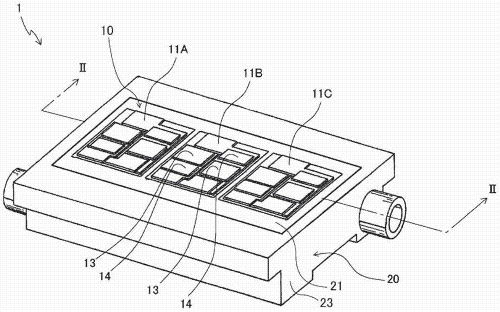
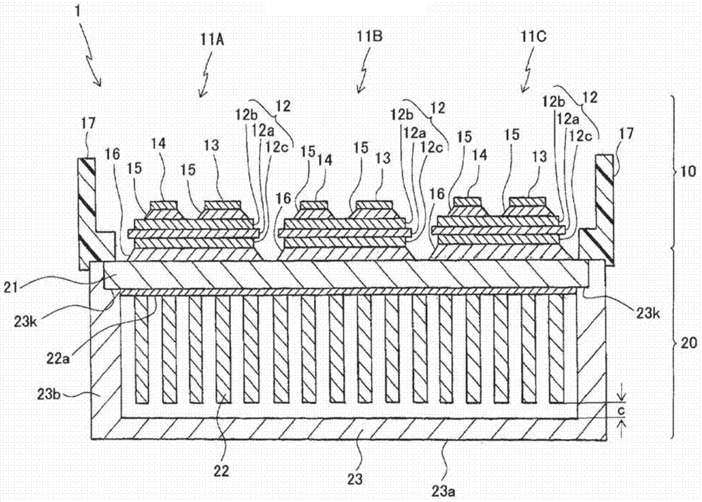
Provided are a semiconductor device wherein heat dissipating characteristics are excellent, reliability is high, and an increase of process cost load is suppressed, and a semiconductor device manufacturing method. A semiconductor device (1) is provided with an insulating substrate (12), semiconductor elements (13, 14), and a cooler (20). The cooler (20) has: a heat dissipating substrate (21) bonded to the insulating substrate (12); a plurality of fins (22) which are provided on the heat dissipating substrate (21) surface on the reverse side of the surface bonded to the insulating substrate (12); and a case (23), which houses the fins (22), and which is provided with an introducing port and a discharge port for a cooling liquid. An end portion of the heat dissipating substrate (21) is disposed in a cutout (23k) that is provided in an upper end portion of a side wall (23b) of the case (23), and the heat dissipating substrate (21) and the case (23) are bonded to each other in a liquid-tight state.
Description
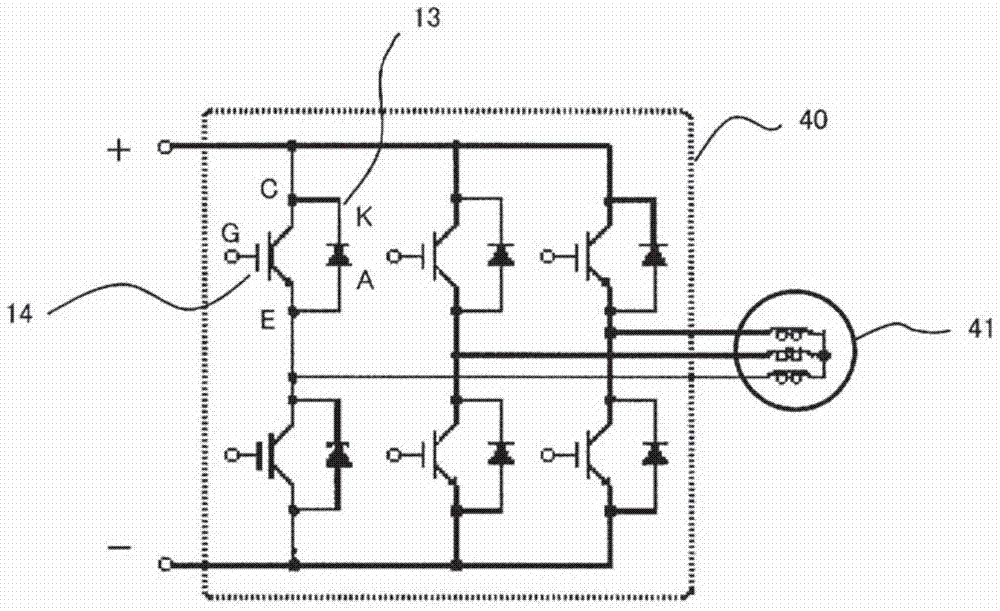
technical field [0001] The present invention relates to a semiconductor device including a cooler for cooling a semiconductor element and a method of manufacturing the semiconductor device. Background technique [0002] In equipment using electric motors such as hybrid vehicles and electric vehicles, power conversion devices are used for energy saving. In this power conversion device, semiconductor modules are widely used. Such a semiconductor module constituting a control device for energy saving includes a power semiconductor element that controls a large current. General power semiconductor elements generate heat when controlling large currents, and the amount of heat generated increases with the miniaturization and higher output of power conversion devices. Therefore, a method of cooling a semiconductor module including a plurality of power semiconductor elements becomes a big problem. [0003] Conventionally, a liquid-cooled cooler is used as a cooler attached to the...
Claims
Login to View More Application Information
Patent Timeline
 Patent Type & Authority Applications(China)
IPC IPC(8): H01L23/473H05K7/20
CPCH01L23/3735H01L2224/32225H01L2924/13055H01L2924/1305H01L2924/351H01L2924/15787H01L23/473H01L2924/00H01L23/12H01L24/81H01L2224/81085
Inventor 乡原广道两角朗山田教文
Owner FUJI ELECTRIC CO LTD
Features
- R&D
- Intellectual Property
- Life Sciences
- Materials
- Tech Scout
- Unparalleled Data Quality
- Higher Quality Content
- 60% Fewer Hallucinations
Learn More Browse by: Latest US Patents, China's latest patents, Technical Efficacy Thesaurus, Application Domain, Technology Topic, Popular Technical Reports.
© 2025 PatSnap. All rights reserved.Legal|Privacy policy|Modern Slavery Act Transparency Statement|Sitemap|About US| Contact US: help@patsnap.com