Method of manufacturing semiconductor device

A manufacturing method and semiconductor technology, applied in the fields of semiconductor/solid-state device manufacturing, semiconductor devices, electric solid-state devices, etc., can solve the problems of decreased mechanical strength of semiconductor wafers, prone to fractures or cracks, and difficult handling.

Inactive Publication Date: 2014-12-31
FUJI ELECTRIC CO LTD
View PDF7 Cites 2 Cited by
  • Summary
  • Abstract
  • Description
  • Claims
  • Application Information

AI Technical Summary

Problems solved by technology

[0004] However, since the mechanical strength of the thinned semiconductor wafer is lowered

Method used


Image

  • Method of manufacturing semiconductor device
  • Method of manufacturing semiconductor device
  • Method of manufacturing semiconductor device

Examples


Embodiment approach

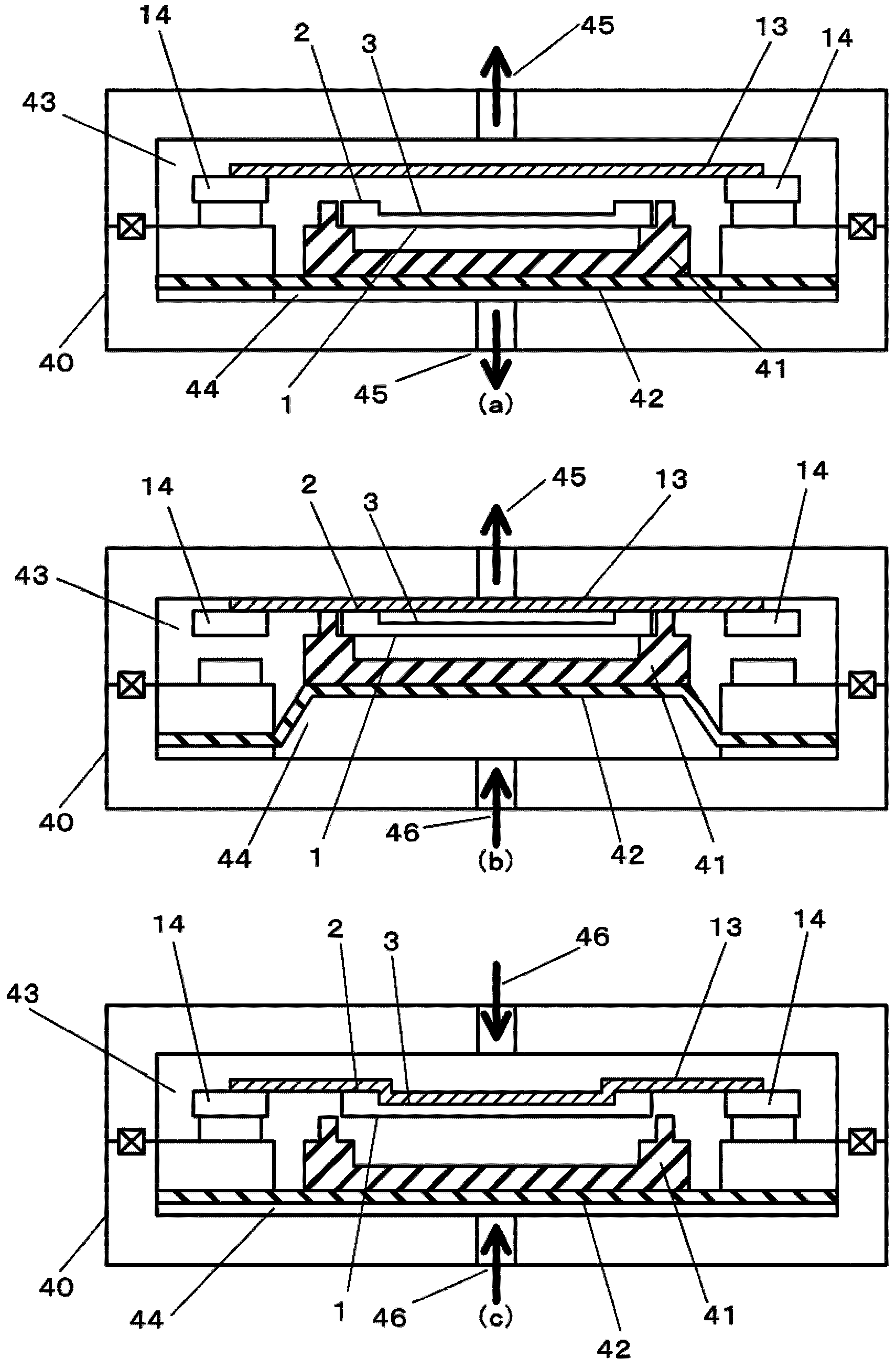
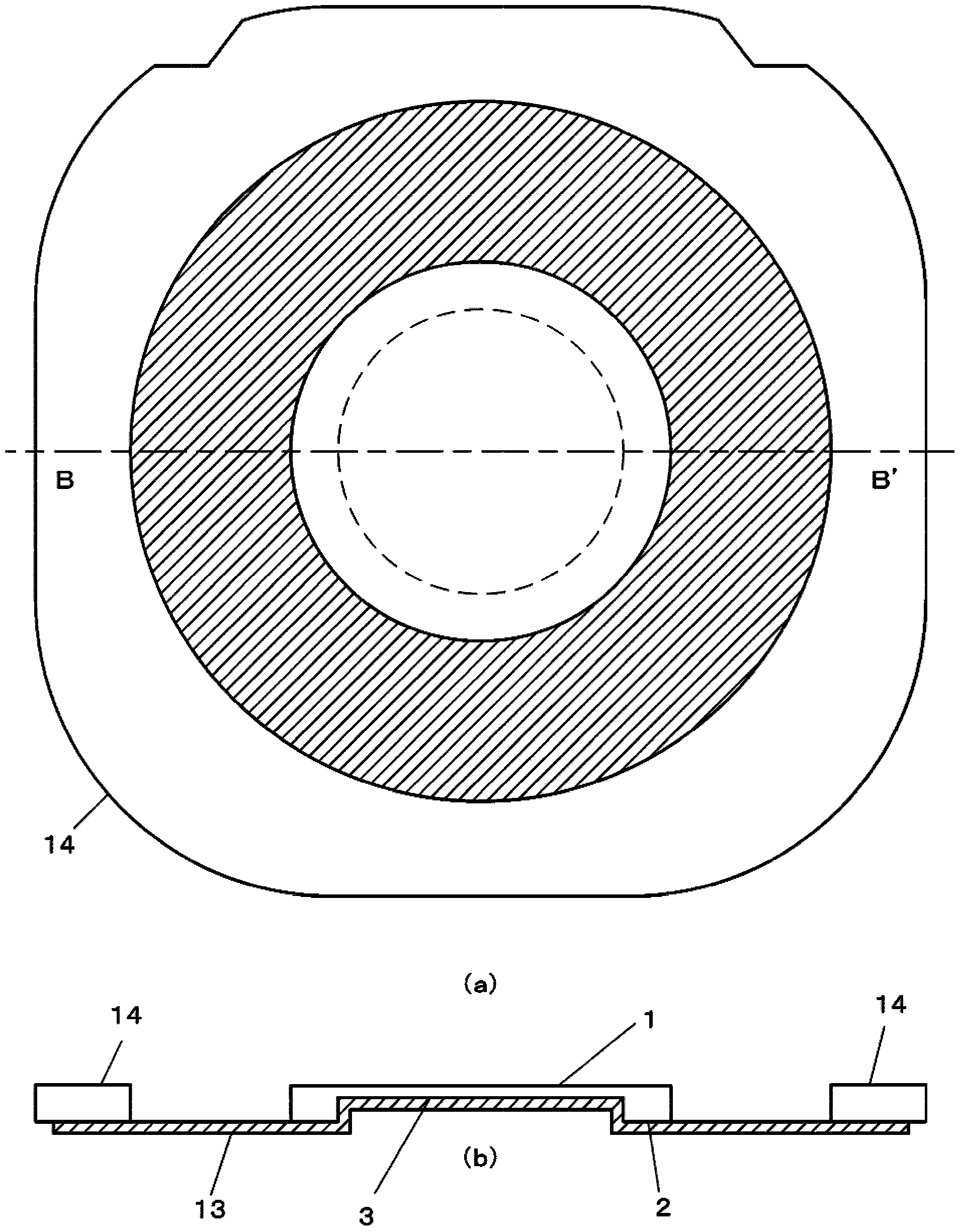
[0046] Figure 18 The semiconductor wafer 1 whose central part is thinned and the outer peripheral part becomes the ring-shaped reinforcing part 2 is shown in . Figure 18 (a) is a top view of a semiconductor wafer 1, Figure 18 (b) is Figure 18 (a) A-A' sectional view.

[0047] Depend on Figure 18 (b) It can be seen that the thick ring-shaped reinforcing portion 2 is formed on the outer peripheral portion of the back surface of the semiconductor wafer 1 , and the thin back surface concave portion 3 is formed on the central portion of the back surface of the semiconductor wafer 1 .

[0048] Depend on Figure 18 (a) It can be seen that the element formation region 6 in which the semiconductor device 4 is formed exists in the rear surface recess 3 , and the chip dividing line 7 is formed in the element formation region 6 for cutting the element formation region 6 to obtain individual semiconductor devices 4 . In addition, the area other than the element formation area 6 in the ...


PUM


Abstract

The invention provides a device for manufacturing a semiconductor device, which can reduce man-hour used for removing a circular enhancement part of a semiconductor chip and reduce cracks or drop of debris. According to the method, a semiconductor chip is divided into a plurality of semiconductor devices; a central section on the back of the semiconductor chip is provided with a recess thinner than the periphery; the periphery is provided with a circular enhancement part; the recess is provided with a semiconductor element area used for forming a plurality of semiconductor devices, and a residual area formed by the recess except the semiconductor element area. The method comprises an installation process in which the back of the semiconductor chip is installed to a cutting support through a bonding belt; a cutting process in which the back of the semiconductor chip on the cutting support is placed to a workbench of a snug smaller than the recess, and a semiconductor element forming area is cut from a front side of the semiconductor chip to cut a plurality of semiconductor devices one by one; a bonding force decline process in which bonding force of the bonding belt is declined; a stripping process in which the circular enhancement part is stripped from the bonding belt; and a removing process in which the circular enhancement part and the residual area are removed.

Description

technical field [0001] The present invention relates to a method of manufacturing a semiconductor device using a semiconductor wafer having a circular concave portion on the back surface. Background technique [0002] In recent years, IGBT (Insulated Gate Bipolar Transistor: Insulated Gate Bipolar Transistor) has been required to have high performance and low cost, so semiconductor wafers have become thinner and thinner. For example, the thickness of the semiconductor wafer needs to be as thin as about 50 μm to 100 μm, or thinner. [0003] The semiconductor wafer is thinned by grinding the back surface of the semiconductor wafer to a predetermined thickness after forming the device structure on the front surface of the semiconductor wafer. [0004] However, since the mechanical strength of the thinned semiconductor wafer is lowered, fractures and cracks are likely to occur, making handling such as transportation difficult. [0005] Thus, after the element structure is form...

Claims


Application Information

Patent Timeline
IPC IPC(8): H01L21/02
CPCH01L21/6836H01L21/78H01L2221/68327
Inventor 田中阳子
Owner FUJI ELECTRIC CO LTD
Why Eureka
Try Eureka