

Manufacturing method of fusing device
A technology of fuses and devices, which is applied in the field of preparation of fuse devices, can solve problems such as diode chip defects, and achieve the effects of reducing the number of times of exposure, eliminating defects, and reducing the number of times of corrosion
Inactive Publication Date: 2014-12-31
SEMICON MFG INT (SHANGHAI) CORP
View PDF3 Cites 4 Cited by
- Summary
- Abstract
- Description
- Claims
- Application Information
AI Technical Summary
Problems solved by technology
For example, the failure of a single metal wire, diode or transistor, etc. can lead to the defect of the entire chip
Method used
View moreImage
Smart ImageViewing Examples

Examples
preparation example Construction
[0036] Combining the above core ideas, the present invention provides a method for preparing a fuse device, comprising the following steps:
[0037] Step S01, providing a substrate, the substrate has a pad area and a fuse area, the pad area has a pad, and the fuse area has a fuse;
[0038] Step S02, preparing a passivation layer on the substrate;
[0039] Step S03 , removing part of the thickness of the passivation layer of the fuse region, so that the passivation layer above the fuse remains to a predetermined thickness;
[0040] Step S04 , selectively removing the passivation layer in the pad region to expose the pad.
Login to View More PUM
 Abstract
The invention discloses a manufacturing method of a fusing device. The manufacturing method comprises the following steps: providing a substrate, wherein the substrate is provided with a welding pad region and a fusing region, the welding pad region is provided with a welding pad, and the fusing region is provided with a fuse; making a passivation layer on the substrate; removing a part of the thickness of the passivation layer of the fusing region till a preset thickness is left for the passivation layer above the fuse; and selectively removing the passivation layer of the welding pad region to expose the welding pad. According to the manufacturing method of the fusing device, the welding pad is not in an exposed state in the step of selective removal of the passivation layer of the welding pad region, so that the exposure times of the welding pad are reduced, the corrosion times of the welding pad are reduced, surface defects of the welding pad are further reduced or eliminated, and the reliability of the device is enhanced.
Description
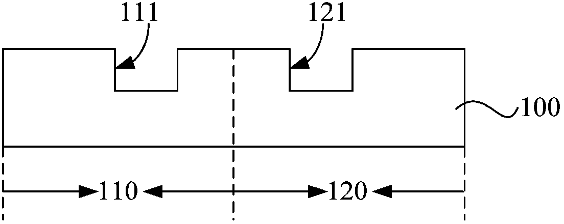
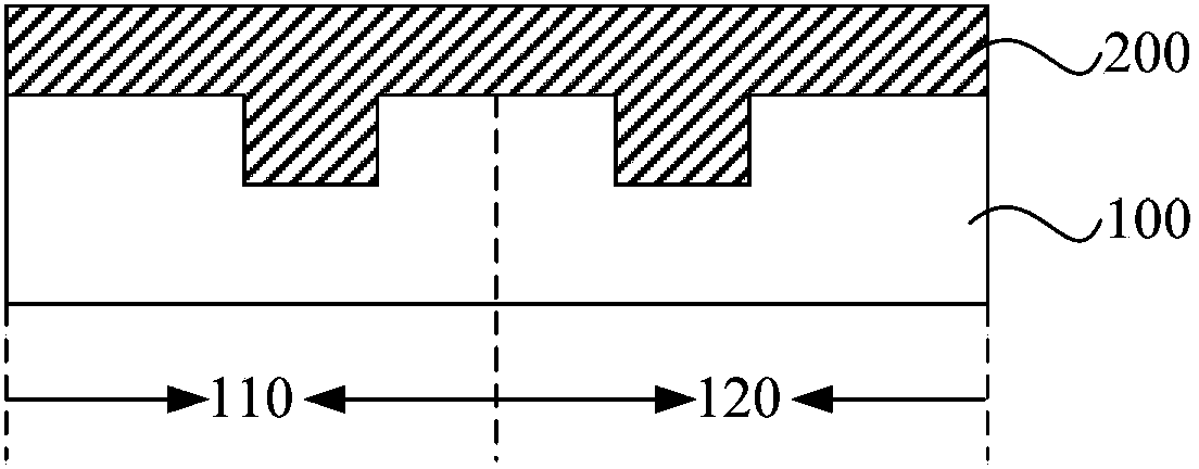
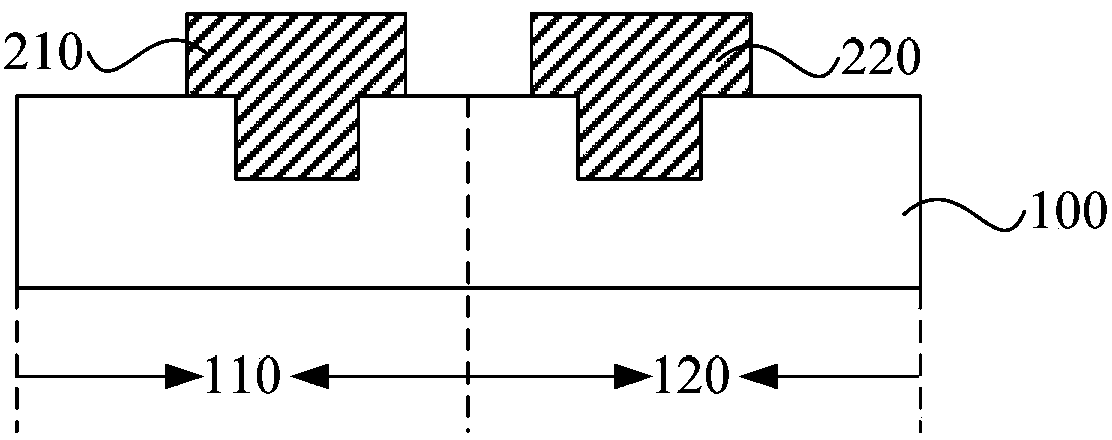
technical field [0001] The invention relates to the technical field of semiconductor manufacturing, in particular to a method for preparing a fuse device. Background technique [0002] With the miniaturization and increase in complexity of semiconductor processes, semiconductor devices become more susceptible to various defects. For example, the failure of a single metal wire, diode, or transistor can lead to a defect in the entire chip. In order to solve the above-mentioned problems, the known technology often forms some fusible connection lines in the integrated circuit, that is, fuses (fuse), so as to ensure the availability of the integrated circuit. [0003] see Figure 1a to Figure 1f , Figure 1a to Figure 1f It is the preparation method of the fuse device in the prior art, specifically as follows: [0004] First, a substrate 100 is provided, which has a pad area 110 and a fuse area 120, such as Figure 1a As shown, the pad area 110 has a pad pattern 111 for prepar...
Claims
Login to View More Application Information
Patent Timeline
 IPC IPC(8): H01L21/768H01L23/525
CPCH01L21/76819H01L23/5256H01L2221/1005
Inventor李志国查源卿
OwnerSEMICON MFG INT (SHANGHAI) CORP