A high-precision wavelength plate wafer processing technology

A wafer processing and high-precision technology, applied in the field of high-precision wavelength plate processing, can solve the problems of inconsistent wafer angles, low efficiency, and many unqualified products, and achieve the effects of easy guarantee of processing accuracy, good angle consistency, and high efficiency

Active Publication Date: 2016-11-16
北京石晶光电科技股份有限公司
View PDF7 Cites 0 Cited by
  • Summary
  • Abstract
  • Description
  • Claims
  • Application Information

AI Technical Summary

Problems solved by technology

[0005] The problem with the above method is that each piece needs to be bonded consistently when sticking the ingot, otherwise the angles of the wafers in the same crystal ingot are inconsistent after cutting, and more unqualified products are likely to appear; meanwhile, the sticking ingot cutting process is cumbersome and inefficient, so This process is only suitable for the processing of low-end wavelength plate wafers with loose angle requirements and a very small number
[0006] Other methods of using an external circular cutting machine to cut the sticky mounds, and then grinding the shape are similar to this principle, but they do not have the advantage of being able to meet mass production and high-precision production

Method used


Image

  • A high-precision wavelength plate wafer processing technology
  • A high-precision wavelength plate wafer processing technology

Examples


Embodiment Construction

[0022] The technical solutions of the present invention will be described in further detail below through specific implementation methods.

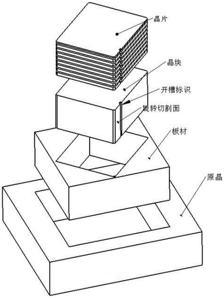
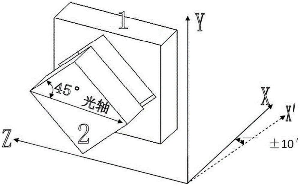
[0023] Such as figure 2 As shown, the raw plate 1 is sliced ​​at the design angle, the slice 2 is the position in the plate, the X, Y, and Z axes are the axial directions of the crystal plate, and the Z axis (optical axis) direction remains unchanged. , the angle between the short edge and the Z-axis (optical axis) is 45° as the design cutting angle, and the angle between the large surface of the wafer and the X-axis is also the design angle. First, the angle between the short edge and the Z-axis (optical axis) After processing, only the angle between the large surface of the wafer and the X-axis is controlled during cutting. The process is simple and easy, and the two angles meet the design angle requirements at the same time.

[0024] The implementation of the inventive production process comprises the following steps:

[0025] Step ...


PUM


Abstract

The invention provides a large-scale processing technology for a precise wavelength plate wafer in a photographic imaging system. The technology comprises the following steps that an original crystal (synthetic quartz crystal, hereinafter referred to as the original crystal) is machined to a plate (synthetic quartz plate, hereinafter referred to as the plate); the angle precision of the plate is controlled well, the plate is rotatably cut, then, precise machining is carried out on the angle of the cutting face, linear cutting machining is carried out on a rotatable crystal block, and the required wavelength plate wafer is obtained. By the adoption of the processing technology, the production efficiency is greatly improved, the quality is stable, the quality and the efficiency of the wafer are higher than the quality and the efficiency of a wafer obtained through traditional lead sticking and then rotary cutting machining and other methods, the production cost is greatly reduced, the efficiency is improved, and the condition is prepared for scale production of the high-precision wavelength plate wafer.

Description

technical field [0001] The invention relates to a technology for processing a high-precision wavelength plate used in a high-definition and high-precision photosensitive imaging system, and in particular relates to a processing technology for processing a high-precision wave plate wafer. Background technique [0002] At present, the main components of the optical low-pass filter and other wafers in the field of electronic information technology and optoelectronic applications are completed in the main processes such as slicing, grinding, and shape processing of artificial quartz crystal blocks with special requirements. Different application fields determine The angles required to cut the wafers are also different. The use of high-precision wavelength plates can convert the light reflected by the photographed object into a perceivable phase difference through the photosensitive imaging system, thereby driving the focusing system to achieve precise focusing, making the photogr...

Claims


Application Information

Patent Timeline
Patent Type & Authority Patents(China)
IPC IPC(8): B28D5/00
CPCB28D5/00
Inventor 邓见会于钦涛朱中晓
Owner 北京石晶光电科技股份有限公司
Why Eureka
Try Eureka