Etching device and method

An etching device, directly above the technology, applied in the direction of electrical components, electrical solid devices, semiconductor/solid device manufacturing, etc., can solve the problems that SiCoNi by-products cannot be completely removed and the output is low, so as to improve the yield and output High, optimize the effect of etching process

Active Publication Date: 2015-01-07
SHANGHAI HUALI MICROELECTRONICS CORP
View PDF5 Cites 1 Cited by
  • Summary
  • Abstract
  • Description
  • Claims
  • Application Information

AI Technical Summary

Problems solved by technology

[0006] In view of the above problems, the present invention provides an etching device and method, through which the etching process in the reaction chamber can be optimized to a certain extent, but only two wafers can be produced. The yield is low, and there is no guarantee that the by-products of the SiCoNi etching process will be completely removed

Method used


Image

  • Etching device and method
  • Etching device and method
  • Etching device and method

Examples


Embodiment Construction

[0034] The present invention will be further described below with reference to the drawings and specific embodiments, but it is not a limitation of the present invention.

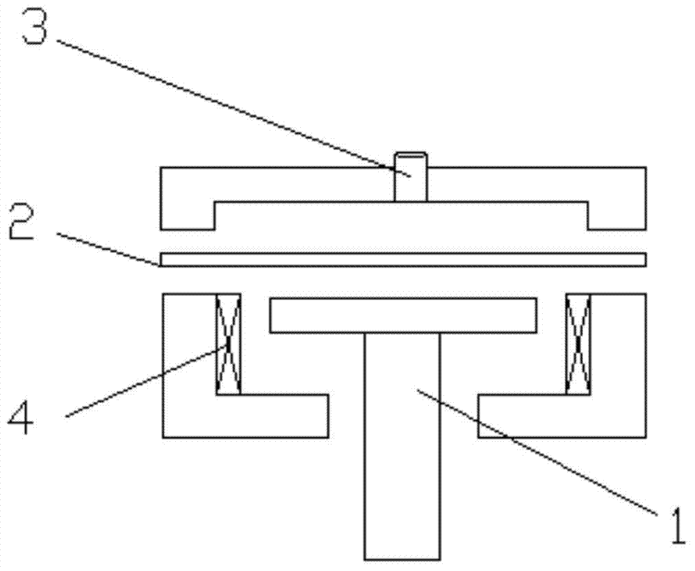
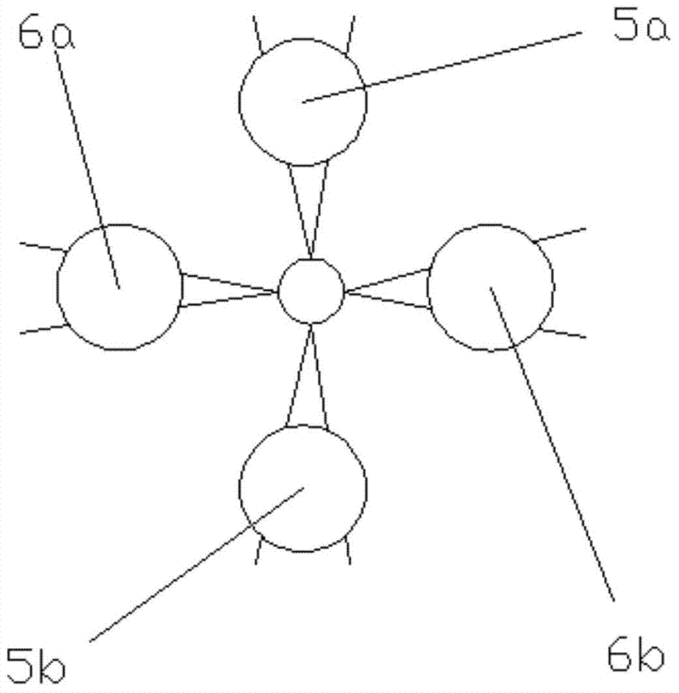
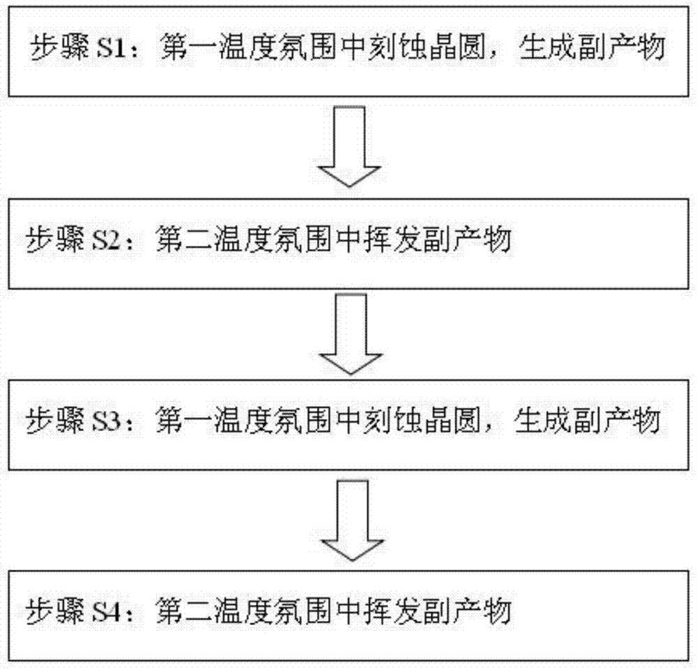
[0035] In order to optimize the etching process of the wafer and simultaneously perform the process production of multiple wafers, and to ensure that the by-products of the SiCoNi reaction chamber during the wafer etching process are completely removed, and the wafer yield rate is improved, the present invention Provide an etching device and method, such as figure 2 with image 3 Shown.

[0036] In the embodiment of the present invention, it relates to an etching device, which is specifically a SiCoNi reaction chamber with a number of pedestals. The SiCoNi etching technology in the reaction chamber is used to remove oxidation on the surface of a wafer. Silicon reduces the contact resistance; in addition, the number of pedestals in the SiCoNi reaction chamber specifically includes: a number of first pedestals, ...


PUM


Abstract

The invention discloses an etching device and method. The etching device is provided with a reaction chamber which comprises a plurality of first substrates and a plurality of second substrates, wherein the first substrates and the second substrates are arranged alternatively. Wafers are conveyed into the reaction chamber, sequentially pass through the first substrate, the second substrate, the first substrate and the second substrate for being processed, and circulate in this way, so that the circulation process of etching, volatilizing, etching and volatilizing of the wafers is finished. Accordingly, the etching process of the wafers is optimized to a great extent, the process production of the multiple wafers can be carried out, the yield is high, it is ensured that by-products generated in the wafer etching process can be removed completely, and the yield of the wafers is greatly increased.

Description

Technical field [0001] The present invention relates to the field of integrated circuit technology, and in particular to an etching device and method. Background technique [0002] The integrated circuit manufacturing process in the prior art uses batch processing technology, that is, a large number of complex multiple devices are formed on the same substrate, and they are connected to each other to have complete electronic functions. The defects caused by any process are all It may lead to failure of circuit production. For example, once the etching by-products in the integrated circuit manufacturing process are not completely removed, it may cause the circuit to open or short. Therefore, in the integrated circuit manufacturing process, how to avoid the occurrence of etching by-products and how to further optimize the etching is a problem that must be paid attention to, especially with the rapid development of integrated circuits, the integration of devices is getting higher an...

Claims


Application Information

Patent Timeline
Patent Type & Authority Applications(China)
IPC IPC(8): H01L21/67H01L21/02
CPCH01L21/02H01L21/67011H01L21/67069H01L2221/67
Inventor 雷通易海兰
Owner SHANGHAI HUALI MICROELECTRONICS CORP
Why Eureka
Try Eureka