Method for electroplating circuit board

A technology for circuit boards and substrates, applied in the directions of printed circuits, printed circuit manufacturing, electrical components, etc., can solve the problems of uneven circuit layout, poor production yield, and difficult to guarantee quality, so as to be beneficial to the etching process and meet the production requirements. requirements, the effect of shortening the production cycle

Inactive Publication Date: 2018-12-07
PEKING UNIV FOUNDER GRP CO LTD +1
View PDF4 Cites 0 Cited by
  • Summary
  • Abstract
  • Description
  • Claims
  • Application Information

AI Technical Summary

Problems solved by technology

However, VCP electroplating will increase surface copper by about 12 μm, resulting in the total copper thickness on the substrate surface exceeding 20 μm after VCP electroplating, and the copper thickness difference on the surface of the board is about 6 μm. The uniform level of copper on the overall surface of the substrate has a great impact on the production of 40 / 40 μm fine lines , mainly manifested in two aspects. On the one hand, when the fine line is etched, the thicker copper on the surface of the circuit board will not be etched completely, resulting in burrs on both sides of the line, and the line spacing is narrow and irregular. On the other hand, the bottom of the circuit board surface Excessive etching of the thinner copper, resulting in etching on both sides of the line, resulting in thinner line width and uneven line layout
It is difficult to guarantee the quality in the whole fine circuit production process, the production yield is poor, or the specifications required by the fine circuit cannot be met at all.

Method used


Image

  • Method for electroplating circuit board
  • Method for electroplating circuit board

Examples


Embodiment Construction

[0016] The following will clearly and completely describe the technical solutions in the embodiments of the present invention with reference to the accompanying drawings in the embodiments of the present invention. Obviously, the described embodiments are only some, not all, embodiments of the present invention. Based on the embodiments of the present invention, all other embodiments obtained by persons of ordinary skill in the art without making creative efforts belong to the protection scope of the present invention.

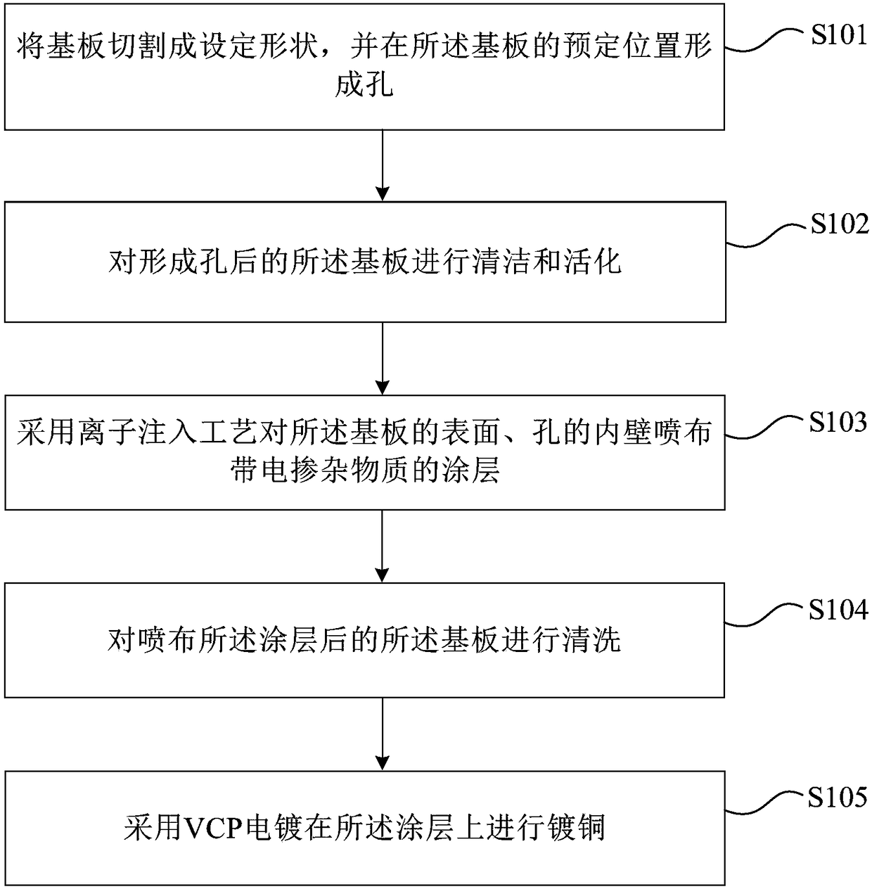
[0017] figure 1 It is a flow chart of the electroplating method for the circuit board provided by the embodiment of the present invention. Such as figure 1 As shown, the embodiment of the present invention provides a method for electroplating a circuit board, and the specific steps of the method are as follows:

[0018] S101 , cutting the substrate into a predetermined shape, and forming a hole at a predetermined position of the substrate.

[0019] In this ...


PUM

PropertyMeasurementUnit
thicknessaaaaaaaaaa
thicknessaaaaaaaaaa

Abstract

The invention provides a method for electroplating a circuit board. After cleaning and activating a substrate after forming holes, the surface of the substrate and the inner walls of the holes are sprayed with a coating of the charged dopant substance by an ion implantation process, the coated substrate is cleaned, and then copper plating is performed on the coating by VCP plating, so that the thickness of the surface copper and the thickness of the hole copper electroplated on the circuit board are uniform, the extreme difference is reduced, the requirements of fine circuit fabrication are satisfied, and the surface copper base meeting requirements is provided for making fine circuit patterns on the circuit board, which is more conducive to the etching process of the circuit board, improves the yield of the product, and also avoids the need for the copper reduction process when the copper surface of the flash plating and VCP plating is too thick. The circuit board production cycle isgreatly shortened and the production cost is lowered.

Description

technical field [0001] The invention relates to the field of circuit boards, in particular to an electroplating method for a circuit board. Background technique [0002] In the PCB dense line process, a mature process with a line width / space (L / S) of 50 / 50 μm has basically been formed in the industry, but there are still many technical barriers in the development of a 40 / 40 μm process. Among them, the fine line Process difficulty In addition to the ultra-precise graphics circuit making (higher developing and etching capabilities are required), there is also a very important factor that requires uniform thin surface copper as the basis of the entire graphics process. Only by controlling a certain surface copper thickness and Only by improving the basis of surface copper uniformity can the feasibility of 40 / 40μm fine line technology development be gradually improved. [0003] The traditional PCB electroplating process adopts the technical combination of flash plating and VCP ...

Claims


Application Information

Patent Timeline
Patent Type & Authority Applications(China)
IPC IPC(8): H05K3/18H05K3/42
CPCH05K3/18H05K3/42H05K2203/092
Inventor 黄得俊车世民陈德福李照飞
Owner PEKING UNIV FOUNDER GRP CO LTD
Why Eureka
Try Eureka