Linear pitch distribution fixed charge island soi withstand voltage structure and power device

A technology of fixed charge island and fixed charge, applied in transistors and other directions, can solve the problem of difficulty in realizing a thin silicon layer of charge island, and achieve the effects of enhanced withstand voltage, simple process realization, and enhanced electric field strength.

Active Publication Date: 2017-08-22
GUILIN UNIV OF ELECTRONIC TECH
View PDF5 Cites 0 Cited by
  • Summary
  • Abstract
  • Description
  • Claims
  • Application Information

AI Technical Summary

Problems solved by technology

Although these interface holes can effectively increase the electric field of the dielectric buried layer and improve the withstand voltage, the charge islands are formed in the silicon active layer, and the lateral and vertical expansion is serious at high temperatures, and it is difficult for the charge islands to form in the thin silicon layer. accomplish

Method used


Image

  • Linear pitch distribution fixed charge island soi withstand voltage structure and power device
  • Linear pitch distribution fixed charge island soi withstand voltage structure and power device
  • Linear pitch distribution fixed charge island soi withstand voltage structure and power device

Examples


Embodiment 1

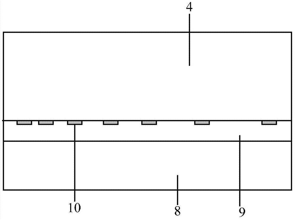
[0034] A linear space distribution fixed charge island SOI withstand voltage structure, such as figure 2 As shown, the withstand voltage structure at least includes a substrate layer 8, a buried dielectric layer 9 and an active layer 4, and the substrate layer 8, buried dielectric layer 9 and active layer 4 are stacked in sequence from bottom to top. The structures of the substrate layer 8 , the dielectric buried layer 9 and the active layer 4 are the same as or similar to the basic structures of existing power devices in the prior art. The material of the active layer 4 can be Si, SiC, GaAs, SiGe, GaN or other semiconductor materials. The material of the dielectric buried layer 9 can be SiO 2 Or a low-k material, where the low-k material (low dielectric constant) can be carbon doped oxide or SiOF. However, the material of the active layer 4 and the material of the buried dielectric layer 9 are not limited to the materials listed above. The above-mentioned buried dielectri...

Embodiment 2

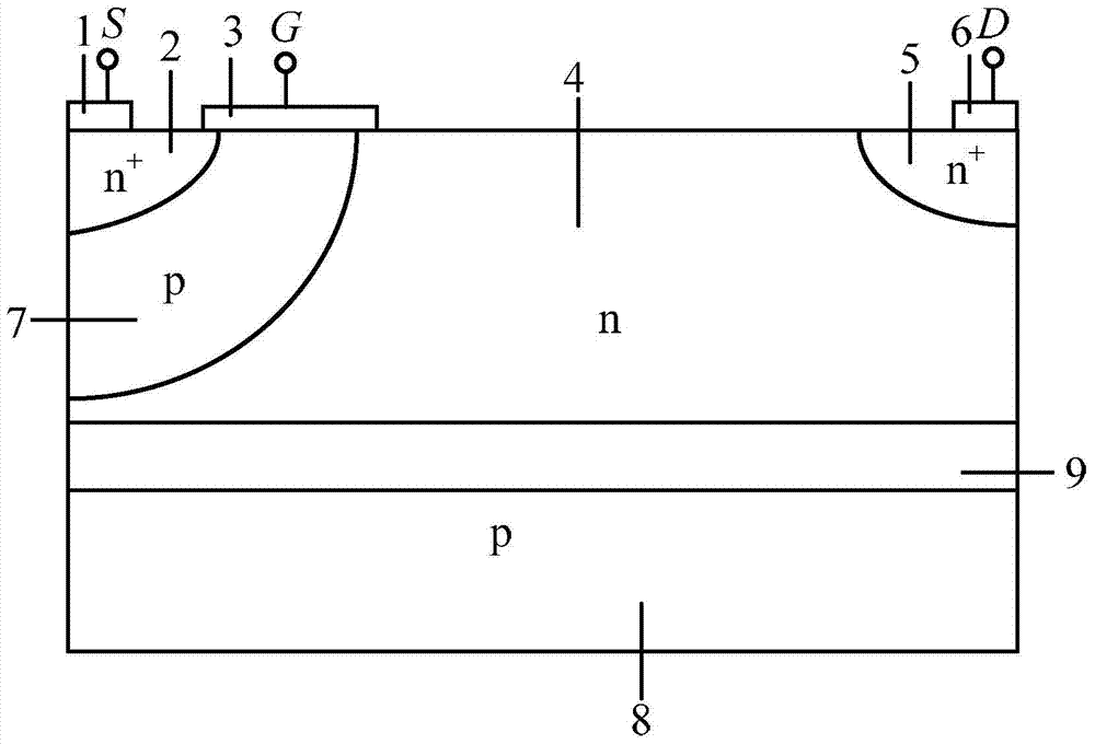
[0039] An SOI power device with a fixed charge island SOI withstand voltage structure distributed in linear intervals, that is, a SOILDMOS device, such as Figure 4 As shown, it includes a substrate layer 8, a dielectric buried layer 9 and an active layer 4 stacked sequentially from bottom to top. An active region 2 , a channel region 7 and a drain region 5 are arranged at upper corners on both sides of the active layer 4 . The source region 2 and the channel region 7 are adjacent to each other, and are arranged at the upper corner of one side of the active layer 4 at the same time. The drain region 5 is disposed at the upper corner of the other side of the active layer 4 . The surface of the active layer 4 is provided with a source 1 , a gate 3 and a drain 6 . The source electrode 1 overlies the source region 2 , and the gate 3 overlies both the source region 2 and the channel region 7 . The drain 6 overlies the drain region 5 . A plurality of high-concentration fixed cha...

Embodiment 3

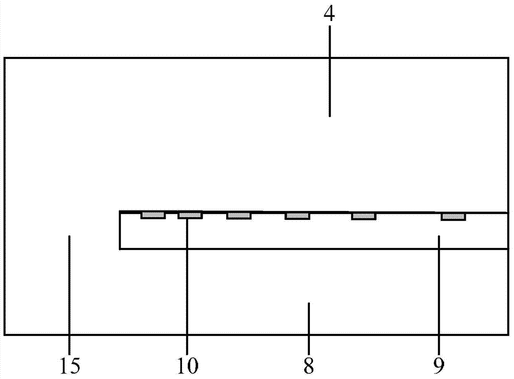
[0043] Another SOI power device with linear pitch distribution fixed charge island SOI withstand voltage structure, that is, SOI IGBT device, such as Figure 7 As shown, it includes a substrate layer 8, a dielectric buried layer 9 and an active layer 4 stacked sequentially from bottom to top. A cathode charge region 12 , a channel region 7 and an anode charge region 13 are provided at upper corners on both sides of the active layer 4 . The cathode charge region 12 is in contact with the channel region 7 and is also arranged at the upper corner of one side of the active layer 4 . The anode charge region 13 is disposed at the upper corner of the other side of the active layer 4 . The surface of the active layer 4 is provided with a cathode 11 , a grid 3 and an anode 14 . The cathode 11 overlies the cathode charge region 12 , and the gate 3 overlies both the cathode charge region 12 and the channel region 7 . The anode 14 overlies the anode charge region 13 . A plurality of h...


PUM


Abstract

The invention discloses a linear space distribution fixed charge island SOI withstand voltage structure and a power device. The SOI withstand voltage structure comprises a substrate layer, a dielectric buried layer, an active layer and a plurality of high-concentration fixed charge areas with the concentration larger than or equal to 1*10<13>cm<-2>, wherein the substrate layer, the dielectric buried layer, the active layer and the high-concentration fixed charge areas are sequentially stacked from bottom to top; the high-concentration fixed charge areas are formed by dielectric materials, and the polarity of charges is positive; the high-concentration fixed charge areas are all located on the upper portion of the dielectric buried layer and arranged interruptedly; in the transverse withstand voltage direction, the space between every two high-concentration fixed charge areas linearly decreases or increases progressively. The electric field of the dielectric buried layer can be greatly improved through the structure, and therefore the withstand voltage can be effectively increased; the technology is easy to obtain and is totally compatible with a conventional CMOS technology.

Description

technical field [0001] The invention belongs to the field of semiconductor power devices, and in particular relates to an SOI pressure-resistant structure and a power device with linearly spaced distribution of fixed charge islands. Background technique [0002] SOI (Silicon On Insulator, silicon on insulating substrate) power devices have high operating speed and integration, reliable insulation performance, strong radiation resistance and no SCR self-locking effect, and are widely used in power electronics, Industrial automation, aerospace and weaponry and other fields. [0003] The breakdown voltage of the SOI power device is calculated by the ionization integration of the electric field along the withstand voltage length, and depends on the smaller of the longitudinal withstand voltage and the lateral withstand voltage. The design principle of SOI lateral withstand voltage can follow the mature silicon-based principles and technologies, such as RESURF (Reduce SURface el...

Claims


Application Information

Patent Timeline
Patent Type & Authority Patents(China)
IPC IPC(8): H01L27/092
Inventor 李海鸥李琦翟江辉唐宁蒋行国李跃
Owner GUILIN UNIV OF ELECTRONIC TECH
Why Eureka
Try Eureka