Semiconductor structure for suppressing harmonic effect and method for forming a structure for suppressing harmonic effect

A harmonic effect, semiconductor technology, applied in the field of suppressing harmonic effects in semiconductor structures

Active Publication Date: 2018-11-20
UNITED MICROELECTRONICS CORP
View PDF4 Cites 0 Cited by
  • Summary
  • Abstract
  • Description
  • Claims
  • Application Information

AI Technical Summary

Problems solved by technology

However, when the RF frequency is selected at a higher frequency, it is more sensitive to the RF harmonic effect induced by parasitic surface charges

Method used


Image

  • Semiconductor structure for suppressing harmonic effect and method for forming a structure for suppressing harmonic effect
  • Semiconductor structure for suppressing harmonic effect and method for forming a structure for suppressing harmonic effect
  • Semiconductor structure for suppressing harmonic effect and method for forming a structure for suppressing harmonic effect

Examples


Embodiment Construction

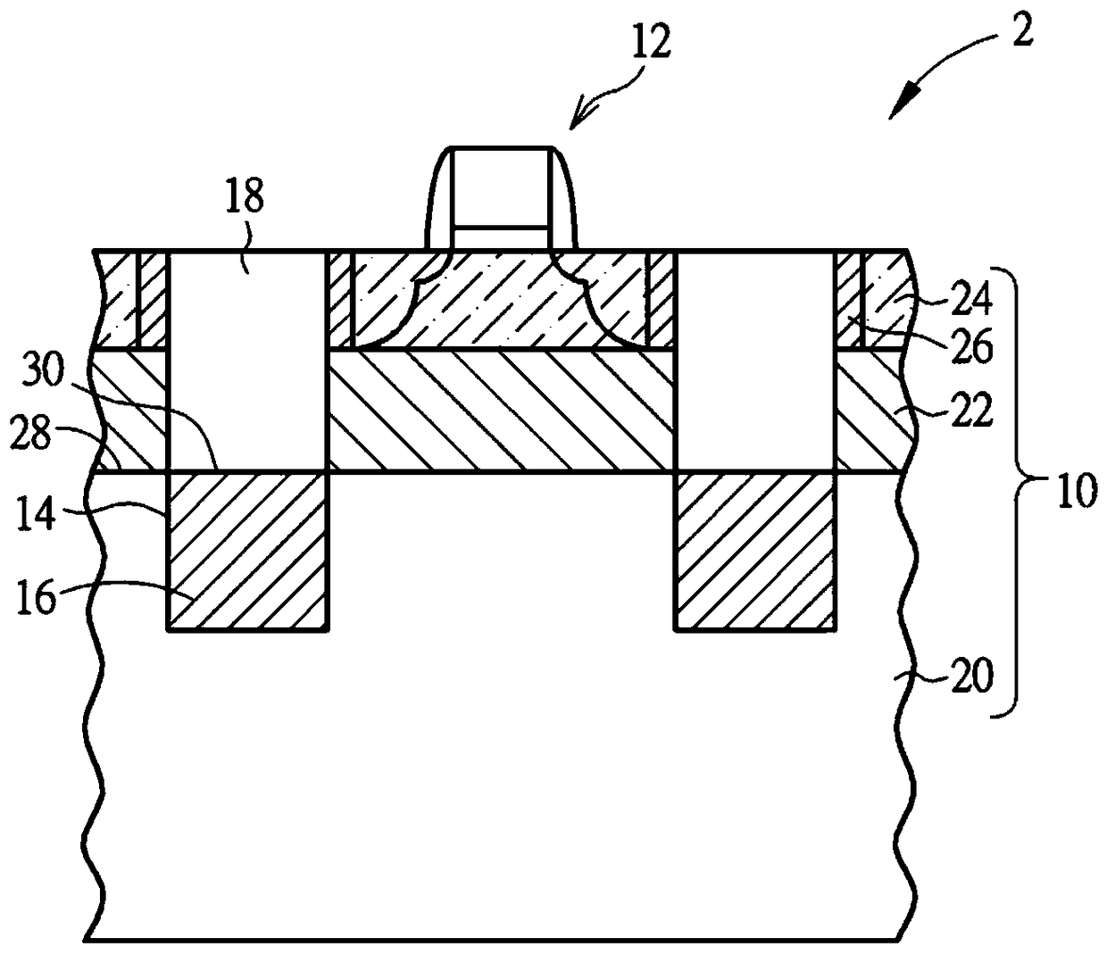
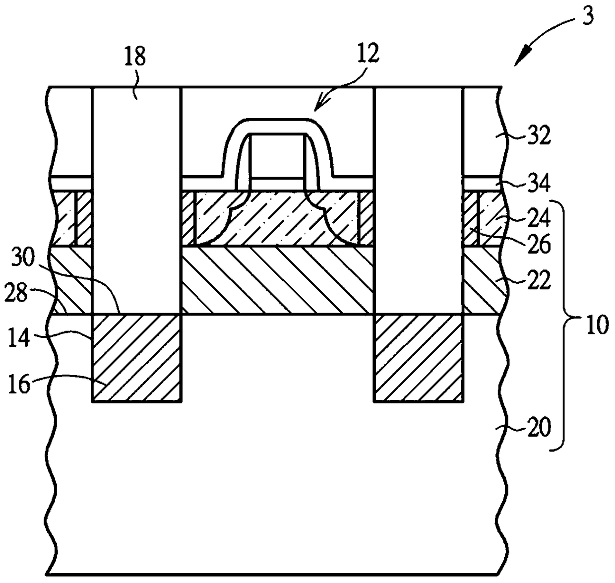
[0023] Figure 1 to Figure 5 A schematic cross-sectional view showing a semiconductor structure capable of suppressing harmonic effects according to several embodiments of several aspects of the present invention. see figure 1 A semiconductor structure 1 capable of suppressing harmonic effects according to an embodiment of the present invention includes a semiconductor substrate 10 , a device 12 , a deep trench 14 , a silicon layer 16 , and a dielectric layer 18 . The semiconductor substrate 10 includes a semiconductor substrate base 20, a buried dielectric layer (buried dielectric) 22 on the semiconductor substrate base 20, a surface semiconductor layer 24 on the buried dielectric layer 22, and a semiconductor layer located in the surface semiconductor layer 24. The shallow trench isolation layer 26. The semiconductor substrate base 20 may include, for example, a high-resistance silicon material such as an amorphous silicon layer or a silicon base with a silicon germanium (...


PUM


Abstract

The invention provides a harmonic effect inhibiting semiconductor structure and a method for forming the same. The semiconductor structure comprises a semiconductor substrate, a device, deep trenches, a silicon layer and a dielectric layer. The semiconductor substrate comprises the components of: a semiconductor substrate base, an embedded dielectric layer, a surface semiconductor layer and a shallow-trench insulating layer in the surface semiconductor layer. The device is arranged on the surface semiconductor layer. The deep trenches are next to the device and extent to the semiconductor substrate base through the shallow-trench insulating layer and the embedded dielectric layer. The silicon layer is arranged at the lower part of the deep trench. The height of the silicon layer is same with or smaller than the height of the top surface of the semiconductor substrate base. The dielectric layer is arranged on the silicon layer in the deep trench. According to the method for forming the harmonic effect inhibiting structure, the semiconductor substrate can be etched before or after formation of an interlayer dielectric layer, thereby forming the deep trenches, and forming the silicon layer in the deep trenches. Carriers or charges can be attracted or captured through the silicon layer, thereby alleviating parasitic surface charges and inhibiting the harmonic effect.

Description

technical field [0001] The invention relates to a semiconductor technology, in particular to a technology for suppressing harmonic effects in semiconductor structures. Background technique [0002] In radio frequency (radio frequency (RF)) IC applications, such as RF switch devices or power amplifier devices, the performance is affected by parasitic surface charges. Harmonic effects are generated due to parasitic surface charges, thereby affecting device performance. Several wafer fabrication techniques are used to solve this problem, such as using a semiconductor-on-insulator (SOI) wafer to isolate the charge from the high resistance wafer substrate. However, when the RF frequency is selected at a higher frequency, it is more sensitive to the RF harmonic effect induced by parasitic surface charges. This problem needs to be solved urgently. Contents of the invention [0003] It is an object of the present invention to provide a semiconductor structure capable of suppres...

Claims


Application Information

Patent Timeline
Patent Type & Authority Patents(China)
IPC IPC(8): H01L29/78H01L21/336H01L27/12H01L21/762
CPCH01L21/762H01L29/06H01L29/66477H01L29/78
Inventor 陈东郁杨国裕
Owner UNITED MICROELECTRONICS CORP
Why Eureka
Try Eureka