Silicon wafer hardness testing device

A hardness test, silicon wafer technology, applied in the direction of testing material hardness, etc., can solve the problems of silicon wafer fragmentation, difficult to grasp manual operation force, inconvenient and laborious, etc., to achieve uniform test pressure, avoid crushing, and accurately measure. Effect

Inactive Publication Date: 2015-01-21
SHANGHAI INTEGRATED CIRCUIT RES & DEV CENT +1
View PDF8 Cites 2 Cited by
  • Summary
  • Abstract
  • Description
  • Claims
  • Application Information

AI Technical Summary

Problems solved by technology

[0005] However, the existing pencil hardness test method needs to manually test the predicted area on the silicon wafer, which is inconvenient and laborious, and the strength of manual operation is not easy to master; in addition, the conventional pencil hardness tester is usually tested by sl

Method used


Image

  • Silicon wafer hardness testing device
  • Silicon wafer hardness testing device

Examples


Embodiment Construction

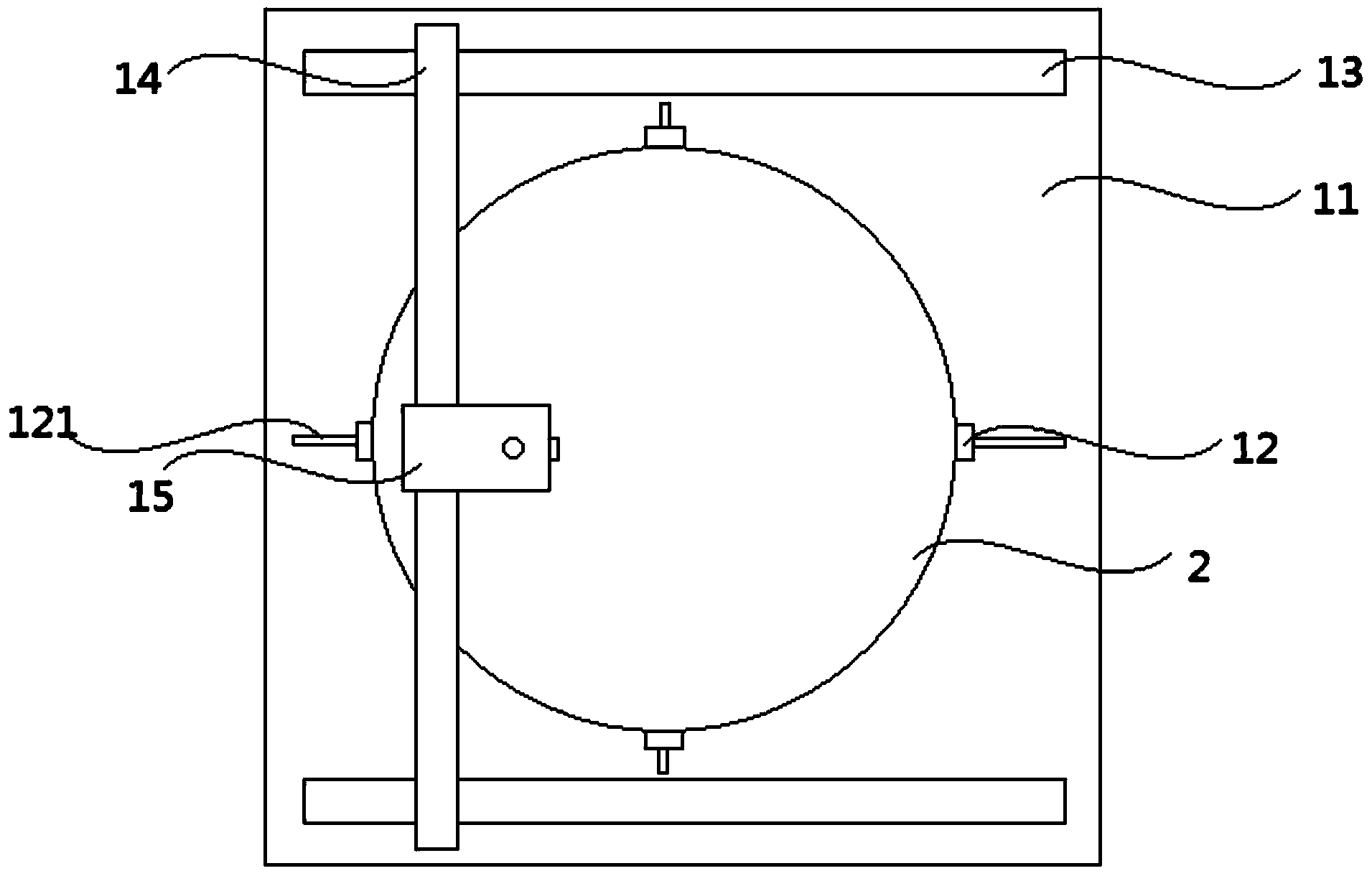
[0026] see figure 1 with figure 2 , the silicon wafer hardness testing device of the present embodiment comprises:

[0027] The test base 11 is used to carry the tested silicon wafer 2;

[0028] Silicon chip holder 12, located on the test base 11, used to clamp and fix the silicon wafer 2 on the test base 11;

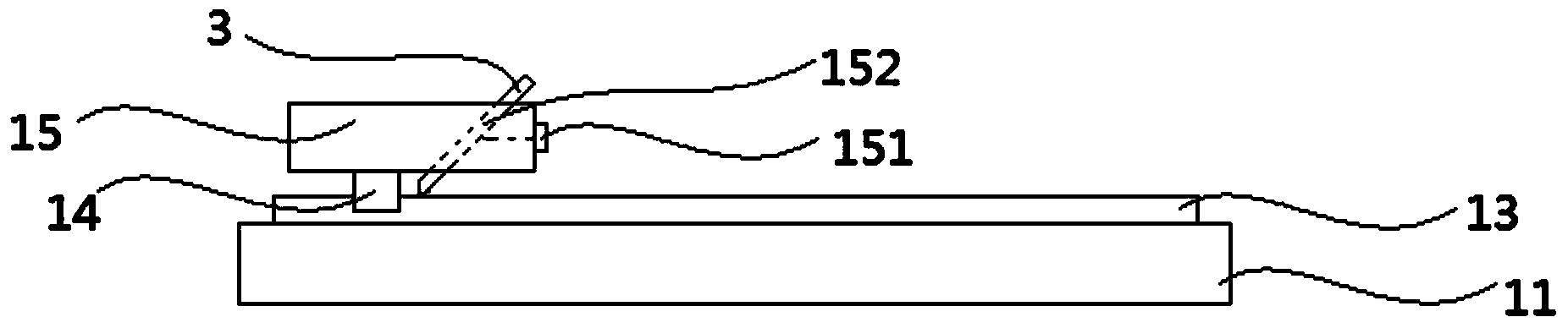
[0029] The transverse track 13 is fixed on the test base 11;

[0030] The longitudinal track 14 is arranged on the transverse track 13 and has a connecting portion slidingly connected with the transverse track 13, so that the longitudinal track 14 can translate along the transverse track 13;

[0031] The pencil test module 15 is arranged on the longitudinal rail 14, and has a connecting portion slidingly connected with the longitudinal rail 14, so that the pencil test module 15 can translate along the longitudinal rail 14. The pencil test module 15 also includes a pencil holder 151 for Clamp and fix different pencils 3 (such as 2H to 9H) to test the hardness of the...


PUM


Abstract

The invention discloses a silicon wafer hardness testing device. According to the silicon wafer hardness testing device, a silicon wafer is fixed on a testing base, and the random movement of a pencil in two-dimensional directions is realized through arranging transverse tracks, a longitudinal track and a pencil testing module, so that a chip of any position on the silicon wafer is subjected to hardness test; the silicon wafer hardness testing device disclosed by the invention has only one point of contact, namely a pencil tip, with the tested silicon wafer, and preferably, the pressure on the silicon wafer applied by the pencil tip is adjusted through a weight or a height adjustment member, so that the testing pressure is even and uniform while the hardness of the silicon wafer is effectively and accurately measured, and the fracture to the surface of the silicon wafer is avoided.

Description

technical field [0001] The invention relates to the field of material hardness testing, in particular to a silicon wafer hardness testing device. Background technique [0002] With the rapid development of large-scale integrated circuits, the quality requirements for silicon wafers are getting higher and higher, and the mechanical strength of silicon materials directly affects the manufacturing yield of silicon wafers and integrated circuits. The high mechanical strength of the silicon material means that the fragmentation rate of the silicon wafer during the slicing, grinding and polishing process is low. cost. [0003] In recent years, the technology of fingerprint sensor products has developed rapidly. Various specifications of fingerprint sensors are used in mobile phones, computers, access control, sign-in machines and other fields, and the surface chips are made of silicon materials. Since the silicon material is a brittle material, the chip surface of the fingerprin...

Claims


Application Information

Patent Timeline
IPC IPC(8): G01N3/40
Inventor 叶红波王勇张悦强
Owner SHANGHAI INTEGRATED CIRCUIT RES & DEV CENT
Why Eureka
Try Eureka