Automatic triggering starting circuit integrating reset function and HMD equipment
An automatic triggering and power-on circuit technology, applied in electrical components, electronic switches, pulse technology, etc., can solve the problems of low power consumption, high power consumption, and no power detection function, and achieve low power consumption and high reliability. Effect
- Summary
- Abstract
- Description
- Claims
- Application Information
AI Technical Summary
Problems solved by technology
Method used
Image
Examples
Embodiment 1
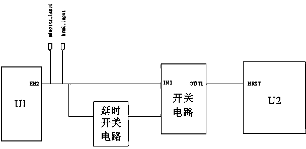
[0024] Embodiment 1, this embodiment proposes an automatic trigger boot circuit with an integrated reset function, such as figure 1 As shown, it includes a power supply device U1 and a control unit U2, and also includes a power supply voltage detection terminal adapter_input for detecting the input voltage of the power supply interface and a multimedia interface voltage detection terminal hdmi_input for detecting the input voltage of the multimedia interface. The voltage detection terminal adapter_input and the multimedia interface voltage detection terminal hdmi_input are respectively connected to the enable signal output end EN2 of the power supply device U1, one of the enable signal output ends EN2 of the power supply device U1 is connected to the control signal input of the switch circuit The control signal output terminal OUT1 of the switch circuit is connected to the reset terminal NRST of the control unit U2, and the enable signal output terminal EN2 of the power supply ...
Embodiment 2
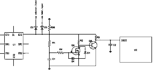
[0027] Embodiment 2, this embodiment provides a specific circuit structure of an automatic trigger power-on circuit integrated with a reset function, such as figure 2As shown, the delay switch circuit in this embodiment includes a first pull-up resistor R1 and a delay circuit, and the delay circuit includes a first capacitor C1 and a fourth resistor R4, and one of the positive poles of the first capacitor C1 is It is connected to the first pull-up resistor R1, and the other path is connected to the gate g of the first NMOS transistor through the fourth resistor R4, the negative electrode of the first capacitor C1 is connected to the ground terminal, and the first NMOS transistor Q9 The source s is connected to the ground terminal, and the drain d is connected to the control signal input terminal of the switch circuit. In this embodiment, a resistor and a capacitor are used to form a delay circuit, and an NMOS transistor Q9 is used as a switch component. When the enable signal...
Embodiment 3
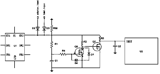
[0034] Embodiment 3, this embodiment provides another implementation circuit of the switching circuit, and the rest of the parts are the same as those recorded in Embodiment 2, and will not be repeated here. The switching circuit of this embodiment includes a second NMOS transistor Q7, so The gate g of the second NMOS transistor Q7 is the control signal input end, connected to the enable signal output end of the power supply device through the second pull-up resistor R2, and the source of the second NMOS transistor is connected to the ground end, so The drain of the second NMOS transistor is a control signal output terminal, one of which is connected to the reset terminal of the control unit, and the other is connected to the enable signal output terminal of the power supply device through the third pull-up resistor R3.
[0035] In order to filter the jitter signal input to the reset terminal NRST of the control unit U2 and prevent misjudgment, the reset terminal NRST also has ...
PUM
 Abstract
Description
Claims
Application Information


