A Tunable Ultra-Wideband Absorber Based on Vanadium Oxide Grating

A technology of vanadium oxide and wave absorbing body is applied in the field of terahertz, which can solve the problems of not wide absorbing frequency band, high cost and high difficulty in preparation, and achieve the effects of simple production, easy construction and stable performance.

Active Publication Date: 2016-06-08
GUILIN UNIV OF ELECTRONIC TECH
View PDF2 Cites 0 Cited by
  • Summary
  • Abstract
  • Description
  • Claims
  • Application Information

AI Technical Summary

Problems solved by technology

In addition, the University of Electronic Science and Technology of China's invention patent "a vanadium oxide composite thin film and its preparation method" published in April 2012 is a material that can be used for terahertz detectors. It consists of two-dimensional vanadium oxide and zero-dimensional fuller It is composed of three components of alkene and one-dimensional carbon nanotubes, which is difficult to prepare
[0007] In short, the performance of the vanadium oxide-based terahertz frequency absorber in the existing reports is not stable enough, the structure is relatively complex, the absorption frequency band is not wide, the absorption rate in the band cannot be adjusted, the cost is high, and it is difficult to be widely used in practice.

Method used


Image

  • A Tunable Ultra-Wideband Absorber Based on Vanadium Oxide Grating
  • A Tunable Ultra-Wideband Absorber Based on Vanadium Oxide Grating
  • A Tunable Ultra-Wideband Absorber Based on Vanadium Oxide Grating

Examples


Embodiment Construction

[0022] The present invention will be described in detail below in conjunction with the accompanying drawings and specific embodiments.

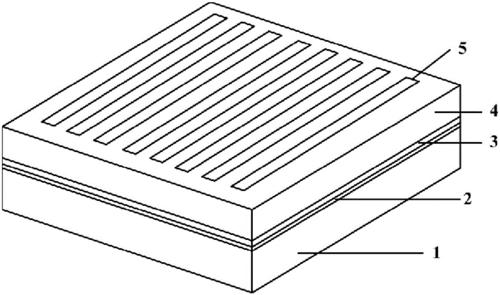
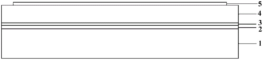
[0023] The embodiment of the tunable ultra-broadband absorber in the terahertz frequency band based on the vanadium oxide grating The structure of an absorber unit is as follows figure 1 and 2 As shown, the lowermost layer is a silicon substrate 1 , and above the silicon substrate are a metal layer 2 , a vanadium oxide layer 3 , a dielectric layer 4 and a vanadium oxide grating 5 .

[0024] In this example, the silicon substrate 1, the metal layer 2, the vanadium oxide layer 3 and the dielectric layer 4 are all squares of 128 microns x 128 microns, and the centers of each layer are on the same straight line, forming a rectangular parallelepiped absorber unit.

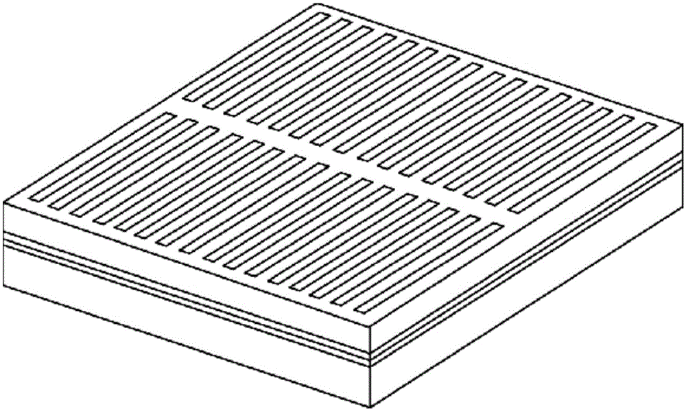
[0025] In this example, each grid bar of the vanadium oxide grating 5 is a rectangular line parallel to the rectangular side of the dielectric layer 4 . The thickness of the bars of ...


PUM

PropertyMeasurementUnit
widthaaaaaaaaaa
thicknessaaaaaaaaaa
thicknessaaaaaaaaaa

Abstract

The invention relates to a terahertz frequency band adjustable ultra-wide band wave absorbing body based on a vanadium oxide grating. The wave absorbing body comprises a silicon substrate, a metal layer, a vanadium oxide layer, a dielectric layer and the vanadium oxide grating, wherein the silicon substrate, the metal layer, the vanadium oxide layer, the dielectric layer and the vanadium oxide grating are sequentially overlapped from bottom to top and are identical rectangles so that a cuboid wave absorbing body unit can be formed. Each grating bar of the vanadium oxide grating is a rectangular line and parallel to the edges of the rectangular dielectric layer, the thickness of the grating bars is 0.2-2 micrometers, the width of the grating bars is 2-20 micrometers, and the center distance is 6-40 micrometers. The length and the width of one wave absorbing body unit are 100-500 micrometers, the metal layer is made of any one of gold, silver, copper and aluminum, the dielectric layer is a polymer layer or a silicon dioxide layer, and the thickness of the dielectric layer is 2-30 micrometers. Multiple wave absorbing body units form an N*N close two-dimensional array, N is larger than or equal to ten, and the length and the width of the array are made to be larger than the transverse diameter of incident terahertz beams. Ultra-wide band absorption and the adjustable absorption rate of the terahertz frequency band are achieved, and the terahertz frequency band adjustable ultra-wide band wave absorbing body is easy to manufacture, low in cost and stable in performance.

Description

technical field [0001] The invention relates to the field of terahertz technology, in particular to a terahertz frequency band tunable ultra-broadband absorber based on a vanadium oxide grating. Background technique [0002] Terahertz waves or THz rays refer to electromagnetic waves with a frequency of 0.1 to 10 THz, between microwaves and infrared. Terahertz waves have strong penetrability and high safety to many dielectric materials and non-polar liquids; Inspection, cell-level imaging, chemical and biological inspection, broadband communication, microwave orientation and many other fields have a wide range of applications. [0003] In the development and utilization of terahertz technology, the detection of terahertz signals is of great significance. Among them, the terahertz detector is one of the core devices of the terahertz system. [0004] Placing the terahertz absorber on the receiving surface of the detector can greatly improve the detection sensitivity and freq...

Claims


Application Information

Patent Timeline
Patent Type & Authority Patents(China)
IPC IPC(8): G01J1/04
Inventor 胡放荣张隆辉王月娥陈涛张丽娟
Owner GUILIN UNIV OF ELECTRONIC TECH
Why Eureka
Try Eureka