Method for detecting defects of 8-inch polished wafers through light-transmitting mirror

A technology of polishing sheet and light-transmitting mirror, which is applied in the direction of optical testing for flaws/defects, etc., to achieve high-sensitivity effects

Inactive Publication Date: 2015-01-28
TIANJIN ZHONGHUAN ADVANCED MATERIAL TECH
View PDF1 Cites 2 Cited by
  • Summary
  • Abstract
  • Description
  • Claims
  • Application Information

AI Technical Summary

Problems solved by technology

Unfortunately, the domestic polishing wafer industry has not been able to apply this te

Method used


Image

  • Method for detecting defects of 8-inch polished wafers through light-transmitting mirror
  • Method for detecting defects of 8-inch polished wafers through light-transmitting mirror

Examples


Embodiment Construction

[0027] The specific embodiments of the present invention will be described in detail below with reference to the accompanying drawings.

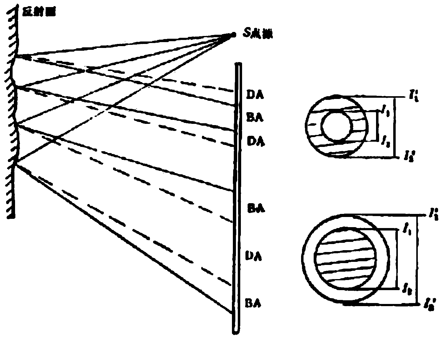
[0028] A method for detecting defects in 8-inch polished sheets with a light-transmitting mirror, the method uses a light-transmitting mirror to detect defects in 8-inch polished sheets, comprising the steps of:

[0029] (1) Turn on the total power input of the test system;

[0030] (2) Turn on the computer;

[0031] (3) Turn on the control box, press the light source power supply switch on the lighting power supply, observe the output ammeter at this time, the current value is 5.4-5.6A, if the displayed value exceeds this range, adjust the output current adjustment knob to adjust the current value to the specified value scope;

[0032] (4) Turn on the imaging display system;

[0033] (5) Turn on the wafer transfer system controller, and place the polished wafer to be tested on the wafer carrier;

[0034] (6) Select test parameters: sele...


PUM

PropertyMeasurementUnit
Thicknessaaaaaaaaaa

Abstract

The invention provides a method for detecting the defects of 8-inch polished wafers through a light-transmitting mirror, wherein in the method, the defects of the 8-inch polished wafers are detected through the light-transmitting mirror. By means of the method, the surface structural properties of the large-area silicon wafers are detected without damage in real time through the light-transmitting mirror, the map of the poor defects of the various silicon wafers is obtained through summarization, and the quality of the monocrystalline silicon wafers is monitored on line.

Description

technical field [0001] The invention relates to a detection method of a polishing sheet, in particular to a method for detecting defects of an 8-inch polishing sheet with a light-transmitting mirror. Background technique [0002] With the rapid development of VLSI technology and various optoelectronic technologies, especially in the production and manufacture of large-scale single crystal silicon wafers, the quality control of materials and devices is more stringent, and a series of problems will be faced. Problems, such as how to detect the surface structure properties of large-area silicon wafers in a non-destructive and real-time manner, how to effectively control the preparation quality of single crystal silicon wafers on-line, etc., only rely on the conventional detection methods in the past, often show extreme Large limitations, it is difficult to meet the requirements of modern detection technology. Therefore, people are still committed to the research and developmen...

Claims


Application Information

Patent Timeline
IPC IPC(8): G01N21/95
Inventor 武卫罗翀王国瑞刘琦闫继增
Owner TIANJIN ZHONGHUAN ADVANCED MATERIAL TECH
Why Eureka
Try Eureka