Array substrate, driving method thereof and display device

A technology of array substrate and drive signal, applied in static indicators, instruments, semiconductor devices, etc., can solve the problems of large resistance, large coupling capacitance, and influence

Inactive Publication Date: 2015-01-28
HEFEI XINSHENG OPTOELECTRONICS TECH CO LTD +1
View PDF6 Cites 18 Cited by
  • Summary
  • Abstract
  • Description
  • Claims
  • Application Information

AI Technical Summary

Problems solved by technology

[0004] The inventors found that for a large-size, high-resolution display device, the resistance of the gate line, the data line, and the common electrode line is large, and the coupling capacitance between the gate line, the data line, and the common electrode is relatively large. When two gate drive circuits drive one gate line at the same time, a row of display thin film transistors is turned on at the same time, and a row of pixel electrodes is charged at the same time, which will pull the voltage of the common electrode to a large extent, thereby affecting the actual voltage applied to the pixel, and prone to afterimages , crosstalk and other bad

Method used


Image

  • Array substrate, driving method thereof and display device
  • Array substrate, driving method thereof and display device
  • Array substrate, driving method thereof and display device

Examples


Embodiment 1

[0036] The embodiment of the present invention provides an array substrate, which can prevent the display thin film transistors controlled by a gate line from being turned on synchronously, thereby reducing the pulling of the common electrode voltage.

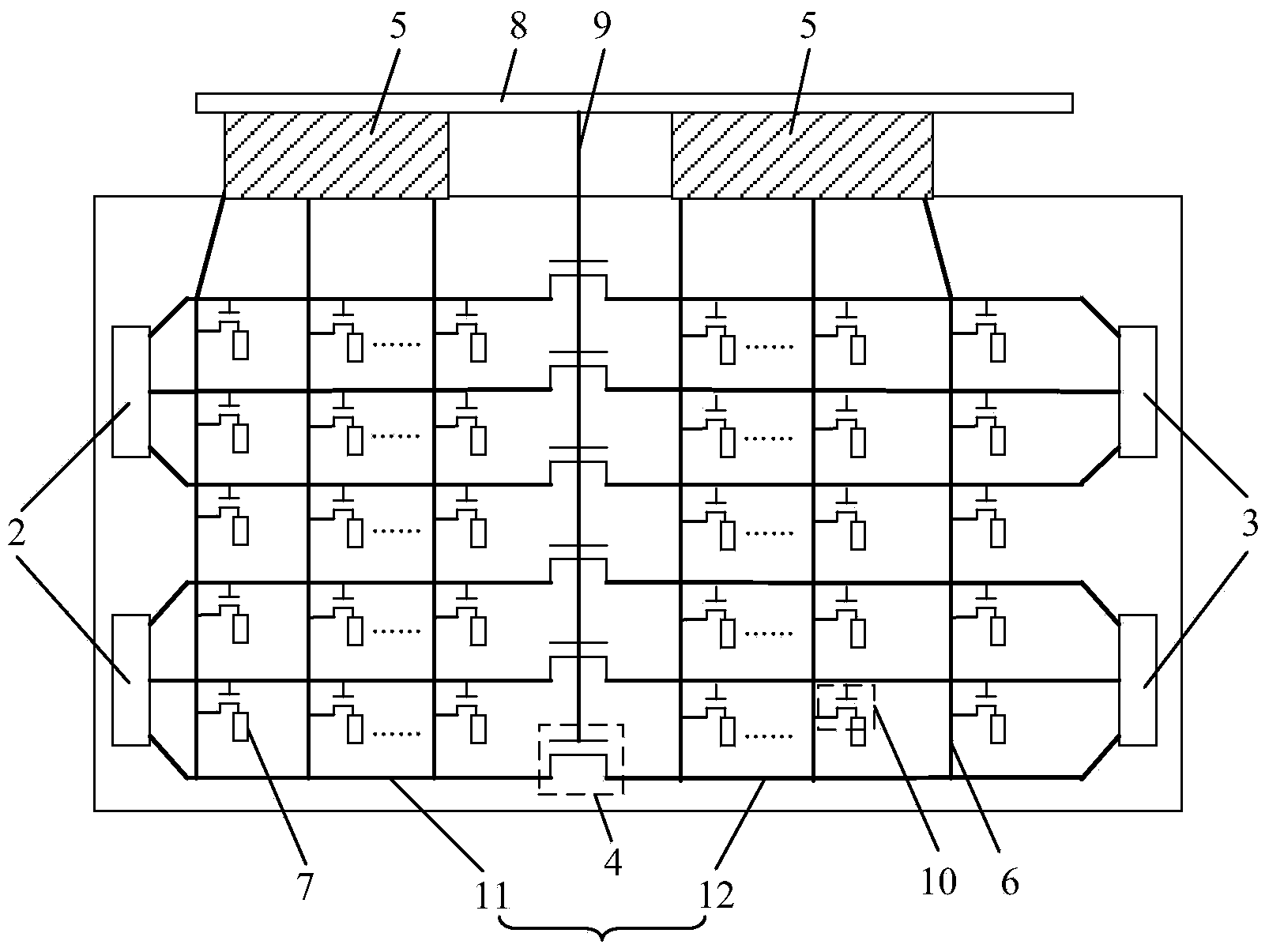
[0037] Specifically, such as figure 1 As shown, the array substrate is provided with a plurality of gate lines 1, the first gate drive circuit 2 and the second gate drive circuit 3 respectively connected to the two ends of the gate line 1, and each gate line 1 is divided into The first gate line part 11 connected to the electrode drive circuit 2 and the second gate line part 12 connected to the second gate drive circuit 3, the switching element 4 is arranged between the first gate line part 11 and the second gate line part 12 .

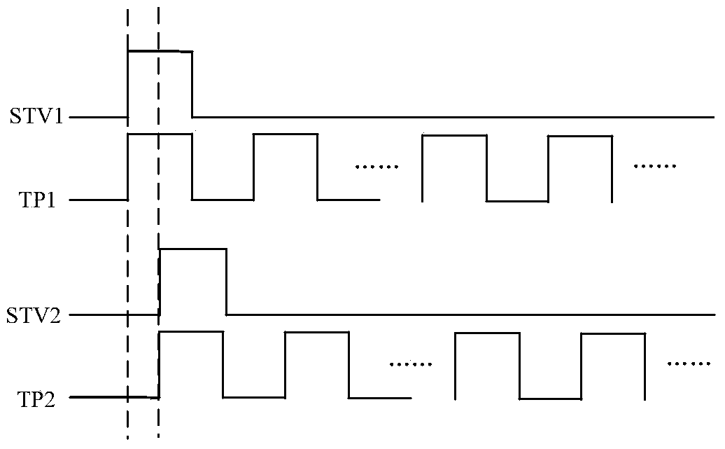
[0038] When the switch element 4 is turned off and the first gate drive circuit 2 drives the first gate line part 11, the first gate drive circuit 2 outputs a gate drive signal to the first gate line ...

Embodiment 2

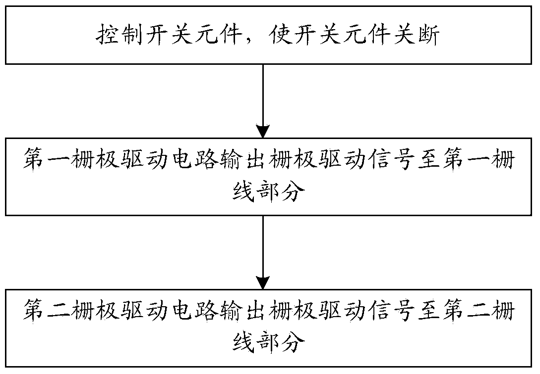
[0048] An embodiment of the present invention provides a driving method for driving the array substrate described in Embodiment 1, specifically, as figure 2 As shown, the driving method includes:

[0049] Step S201, controlling the switch element to turn off the switch element.

[0050] When the switching element 4 is turned off, when the first gate drive circuit 2 drives the first gate line part 11, the first gate drive circuit 2 outputs a gate drive signal to the first gate line part 11, so that the first gate line part The display thin film transistor 10 controlled by 11 is turned on, and the data signal output by the source driver circuit 5 to the data line 6 is transmitted to the pixel electrode 7 through the display thin film transistor 10, so that the display thin film transistor 10 controlled by the first gate line part 11 is connected to The pixel electrode 7 is charged, because the switch element 4 provided between the first gate line part 11 and the second gate li...


PUM


Abstract

The embodiment of the invention discloses an array substrate, a driving method of the array substrate and a display device, and relates to the technical field of display. Display thin film transistors controlled by a grid line can be prevented from being started on synchronously, and then pulling to a public electrode voltage is reduced. A plurality of grid lines are arranged on the array substrate. The two ends of each grid line are connected with a first grid drive circuit and a second grid drive circuit respectively, and each grid line is divided into a first grid line portion connected with the first grid drive circuit and a second grid line portion connected with the second grid drive circuit, wherein a switch element is arranged between the first grid line portion and the second grind line portion.

Description

technical field [0001] The present invention relates to the field of display technology, in particular to an array substrate, a driving method thereof, and a display device. Background technique [0002] The array substrate of the display device is provided with criss-cross gate lines and data lines. The gate lines and data lines enclose pixels, and the pixels are provided with display thin film transistors and pixel electrodes. One gate line controls the opening of a row of display thin film transistors, thereby determining Whether the data line charges the pixel electrode of the row of pixels, therefore, in order to drive the display device, a gate drive circuit and a source drive circuit need to be provided on the array substrate, wherein the gate drive circuit outputs a gate drive signal to the gate line, The source driving circuit outputs data signals to the data lines. [0003] At present, display devices are developing in the direction of large size and high resoluti...

Claims


Application Information

Patent Timeline
Patent Type & Authority Applications(China)
IPC IPC(8): G09G3/20
CPCG09G3/20G09G2310/0267G02F1/136286H01L27/124G09G3/2096G09G2300/0408G09G2300/08G09G2310/0213G09G2310/08G09G2320/0209G09G2320/0257G09G2330/026
Inventor 王慧梁恒镇
Owner HEFEI XINSHENG OPTOELECTRONICS TECH CO LTD
Why Eureka
Try Eureka