Sealant encapsulation structure of automotive electronic elements and sealant sealing method thereof

An electronic component and glue sealing technology is applied in the structural field of automotive electronic component sealant encapsulation modules, which can solve the problems of increased manufacturing difficulty, leakage failure, and high design requirements, and achieves simple manufacturing and assembly process, guaranteed installation position, and simplified structure. small effect

Active Publication Date: 2015-01-28
UNITED AUTOMOTIVE ELECTRONICS SYST
View PDF7 Cites 7 Cited by
  • Summary
  • Abstract
  • Description
  • Claims
  • Application Information

AI Technical Summary

Problems solved by technology

Assembled packaging has high requirements on the performance of the seal and the accuracy of the two connected parts. It is prone to leakage and failure in the harsh and harsh application environment of automobiles. For example, the assembly packaging structure with the publication number CN 2896225Y In the actual application process, there have been problems of leakage failure
The connection structure of ultrasonic and laser welding has high design requirements and high production costs
In addition, there are some products that require high installation accuracy, and at the same time require high precision for the parts assembled with each other, so the manufacturing difficulty is greatly increased
[0005] In addition to injection molding and assembly connection packaging methods, a small number of automotive electronic components on the market currently use one-time glue-filling packaging. This one-time glue-filling packaging method is prone to internal stress after the glue is cured due to the direct contact between the glue and the electronic components. Electronic components fail or are at risk of potential failure, such as figure 1 The publication number shown is the invention patent product of CN101008660A. The sealing glue poured to connect the bracket and the shell is easy to flow and cover the electronic components on the circuit board during the curing process. After curing, internal stress will cause the electronic components to fail. This failure is in practice. The performance is more obvious in the high-temperature shock and high-frequency vibration environment of the car
At the same time, one-time glue filling in irregular spaces is prone to inaccurate and uneven filling, which will cause defects on the product surface or internal cavities after curing, so that the product is prone to water, oil, and air leakage problems

Method used


Image

  • Sealant encapsulation structure of automotive electronic elements and sealant sealing method thereof
  • Sealant encapsulation structure of automotive electronic elements and sealant sealing method thereof
  • Sealant encapsulation structure of automotive electronic elements and sealant sealing method thereof

Examples


Embodiment Construction

[0046] The present invention will be further described in detail below in conjunction with the accompanying drawings and specific embodiments.

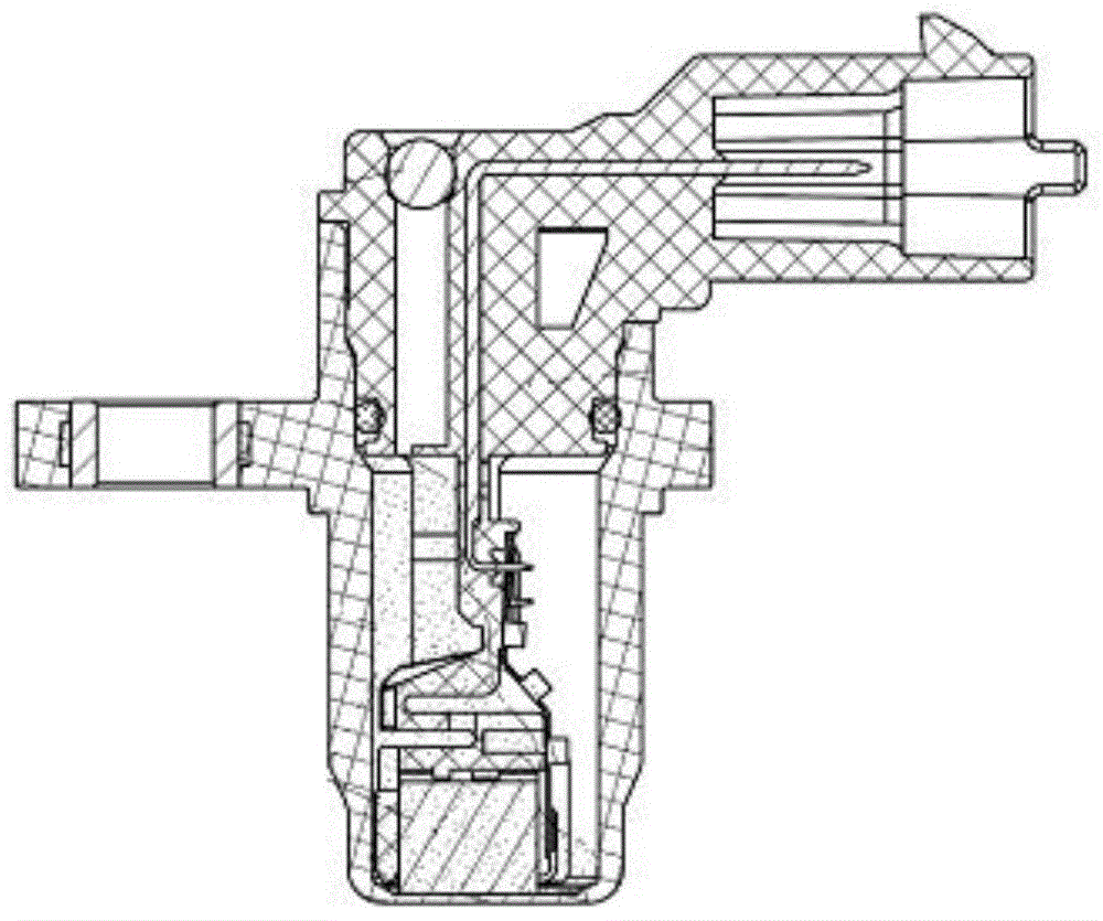
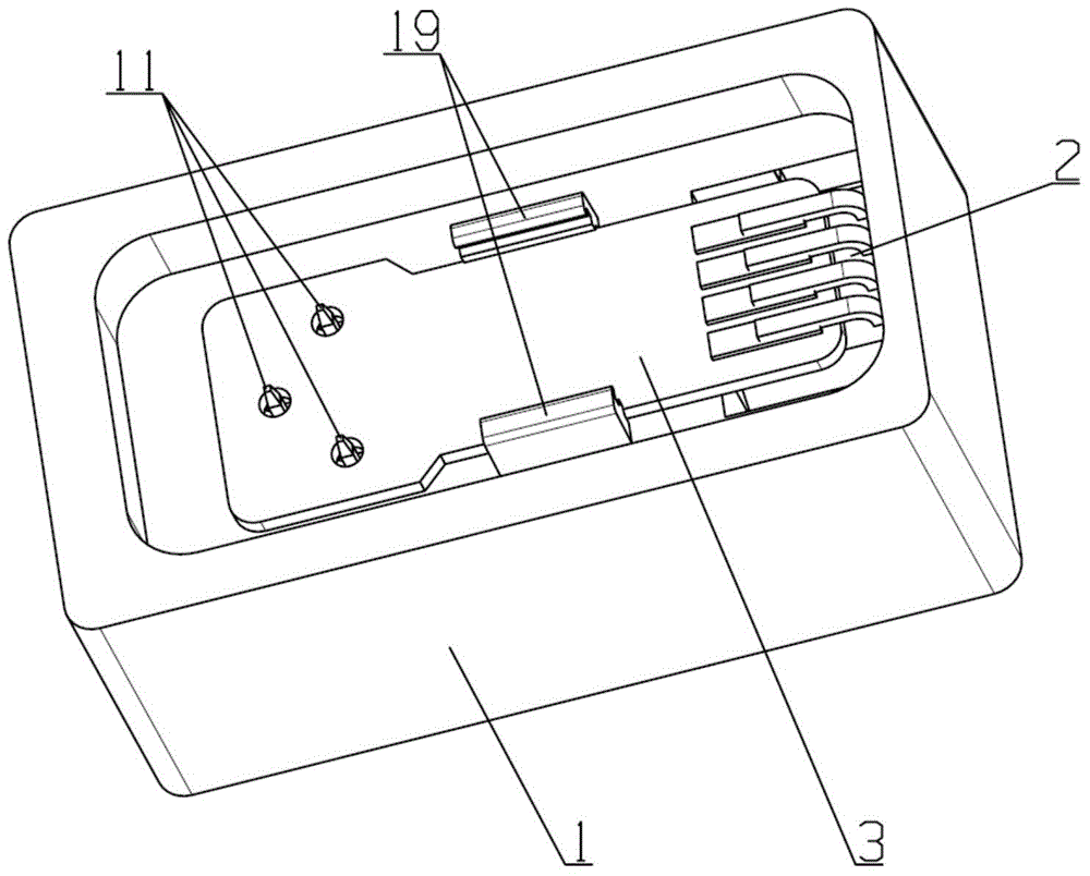
[0047] The sealant encapsulation structure of the vehicle electronic component provided by the present invention, such as figure 2 As shown, it includes a main body 1 , a chip 2 (in this embodiment, a Hall chip is taken as an example for illustration) and a circuit board 3 .

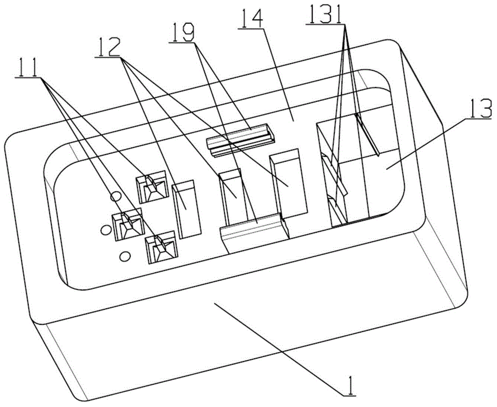
[0048] Such as image 3As shown, the main body 1 is packaged with a PIN pin set 11 by injection molding. The main body 1 is formed with a cavity 14 , and an electronic element cavity 12 and a chip cavity 13 are formed in the cavity 14 . In this embodiment, there are three electronic component cavities 12 and one chip cavity 13 in the concave cavity 14 .

[0049] The chip 2 has a sensor element 21 and a chip PIN pin group 22, such as Figure 4 shown. In this embodiment, taking the sensing element 21 located at the head of the chip 2 as an example, the fixed ...


PUM


Abstract

The invention discloses a sealant encapsulation structure of automotive electronic elements and a sealant sealing method thereof. The sealant encapsulation structure comprises a chip, a circuit board and a main body; the chip comprises a sensing element and a chip pin group; the circuit board comprises a substrate, a second connecting portion, a first connecting portion and the electronic elements; a pin group is formed inside the main body in an injection molding mode; a concaved chamber is formed in the main body; electronic element chambers and a chip chamber are formed in the concaved chamber; the chip is arranged in the chip chamber; the circuit board is arranged in the concaved chamber of the main body; the bottom surface of the substrate is attached to the bottom surface of the concaved chamber; every electronic element is inserted into the corresponding electronic element chamber; the second connecting portion is connected with the chip pin group; the first connecting portion is connected with the pin group of the main body; the sealant is injected into the concaved chamber twice, the sealant covers the circuit board and the natural high temperature curing is performed during first sealant injection, and the concaved chamber is filled with the sealant and the vacuum pumping high temperature curing is performed during second sealant injection. According to the sealant encapsulation structure of the automotive electronic elements and the sealant sealing method thereof, the damage to the electronic elements due to the high temperature curing due to the fact that the sealant flows into the electronic element chambers to cover the electronic elements can be effectively prevented, meanwhile the chip installation position is accurate, the sealing performance is good, the structure is simple, and the cost is low.

Description

technical field [0001] The invention is related to the packaging structure after circuit board chips are connected and assembled, and in particular relates to the structure of a sealing glue packaging module for electronic components used in vehicles. The structure can be used for electronic components such as automotive sensors and electronic actuators. Background technique [0002] At present, there are mainly two types of connection and packaging methods for circuit boards and chips in electronic components such as automotive sensors and electronic actuators: injection molding and assembly. [0003] The injection molding packaging method is to connect the circuit board, the chip and the PIN pin or the wiring harness including the connector together and fix them on the primary injection molding block to form a primary injection molding component, and then form a complete electronic product through secondary injection molding. Due to the high pressure and high temperature o...

Claims


Application Information

Patent Timeline
Patent Type & Authority Applications(China)
IPC IPC(8): H01L23/31H01L23/29H01L21/56
Inventor 何元飞程捷
Owner UNITED AUTOMOTIVE ELECTRONICS SYST
Why Eureka
Try Eureka