LED filament

A LED filament and chip technology, applied in semiconductor devices, electrical components, circuits, etc., can solve the problems of blue leakage of filament devices, large amount of materials, high cost, etc., achieve the effect of no leakage and reduce material costs

Inactive Publication Date: 2015-01-28
SHENZHEN REFOND OPTOELECTRONICS
View PDF5 Cites 10 Cited by
  • Summary
  • Abstract
  • Description
  • Claims
  • Application Information

AI Technical Summary

Problems solved by technology

[0003] Existing LED filament products made of transparent substrates such as sapphire and glass need to mold fluorescent glue around the transparent substrate filament or double-sided dispensing on the front and back of the transparent substrate filament in order to achieve f

Method used


Image

  • LED filament
  • LED filament
  • LED filament

Examples


Embodiment Construction

[0014] The present invention will be described in detail below in conjunction with the accompanying drawings and specific embodiments.

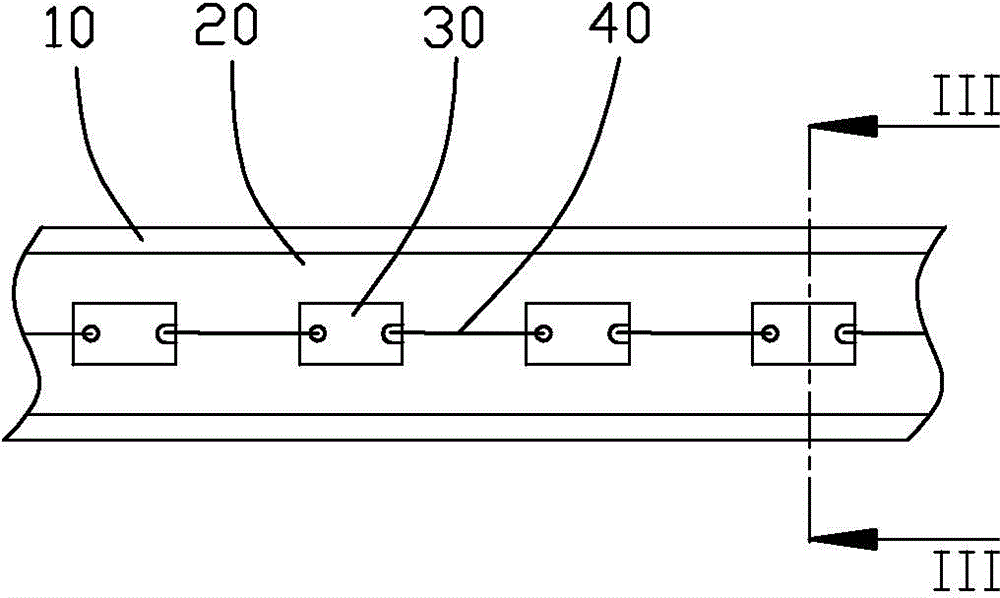
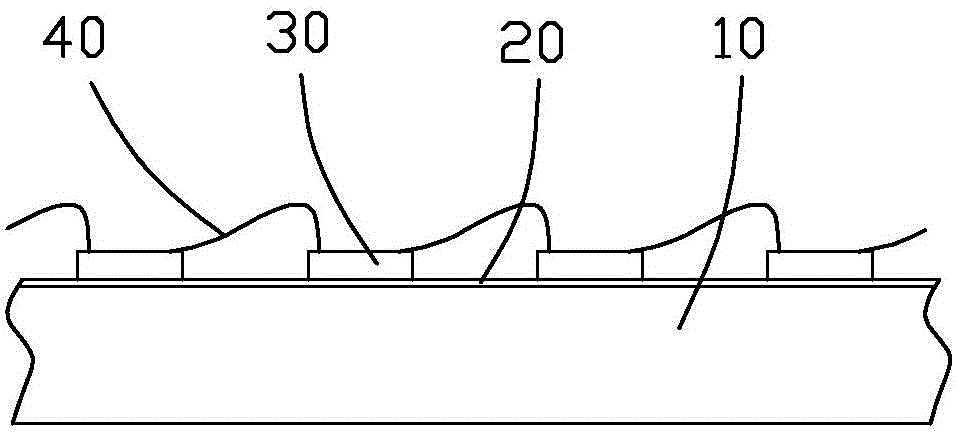
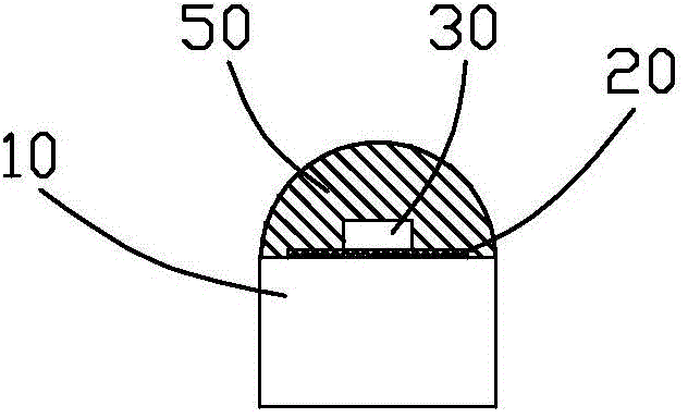
[0015] like figure 1 , figure 2 ,and image 3 As shown, the LED filament of the present invention includes a substrate 10 , a fluorescent glue layer 20 , an LED chip 30 , a wire 40 , and a fluorescent glue coating layer 50 .

[0016] The substrate 10 can be a transparent substrate made of sapphire, high polymer, ceramics or glass, etc., and the fluorescent adhesive layer 20 is formed on the side of the substrate 10 used for crystal bonding by physical and chemical methods. Adhesive layer 20 is a mixture of silica gel, epoxy resin or other viscous substances and fluorescent powder, with a thickness of more than 0.03mm, and its area may be equal to or smaller than the area of ​​one side of the substrate 10 for die bonding, so as to completely or partially cover the substrate 10 for die bonding side. In this embodiment, the area of ​​the fl...


PUM

PropertyMeasurementUnit
Thicknessaaaaaaaaaa

Abstract

An LED filament comprises a transparent substrate and LED wafers arranged on the transparent substrate. The LED wafers are electrically connected through metal wires to form a closed circuit, a fluorescent adhesive layer is formed in a physical or chemical mode on one wafer fixing side of the substrate, the LED wafers are fixedly arranged on the fluorescent adhesive layer and completely located within the range of the fluorescent adhesive layer, and a fluorescent adhesive coating layer is formed on the wafers in an adhesive dispensing or die pressing mode and completely wraps the LED wafers and the wires. According to the LED filament, the wafers are fixedly arranged on the fluorescent adhesive layer formed on the wafer fixing side of the transparent substrate, the fluorescent adhesive coating layer is formed on the wafers in an adhesive dispensing or die pressing mode, the dosage of fluorescent powder and adhesive can be reduced, and the material cost is reduced; and the side of the filament is free of blue leakage.

Description

technical field [0001] The invention relates to LEDs, in particular to LED filaments that emit light at all angles of 360°. Background technique [0002] LED filaments can achieve 360° full-angle light without the need for additional optical devices such as lenses, and can be applied to lighting products such as crystal chandeliers, candle lights, bulb lights, wall lights, etc., bringing unprecedented lighting experience. [0003] Existing LED filament products made of transparent substrates such as sapphire and glass need to mold fluorescent glue around the transparent substrate filament or double-sided dispensing on the front and back of the transparent substrate filament in order to achieve full-circle light emission. Fluorescent glue or fluorescent glue on both sides of the substrate, the process is cumbersome, the material consumption is large, the cost is high, and the side of the filament device with double-sided glue on the substrate is prone to blue leakage. Conte...

Claims


Application Information

Patent Timeline
IPC IPC(8): H01L33/50H01L25/075
CPCH01L25/075H01L33/502H01L33/56H01L2933/005H01L2933/0041H01L2224/48091H01L2224/48137H01L2224/48465H01L2224/48471H01L2924/00014H01L2924/00
Inventor 晏思平游志
Owner SHENZHEN REFOND OPTOELECTRONICS
Why Eureka
Try Eureka