Chip pin shaping device and method based on laser thermal stress forming

A shaping device and thermal stress technology, applied in the manufacturing of electrical components, electric solid-state devices, semiconductor/solid-state devices, etc., can solve the problem of difficult control of consistency accuracy, meet the requirements of consistency tolerance, increase investment, and have high shaping efficiency Effect

Active Publication Date: 2015-02-04
BEIJING GUOWANG OPTICAL TECH CO LTD
View PDF4 Cites 2 Cited by
  • Summary
  • Abstract
  • Description
  • Claims
  • Application Information

AI Technical Summary

Problems solved by technology

[0004] In order to overcome the defects of the prior art that the consistency accuracy of pin correction is not easy to control, the present invention provides a chip pin shaping device and method based on laser thermal stress forming technology, combined with non-contact displacement measurement technology, it can realize DIP packaging IC The highly consistent non-contact modeless correction of chip pins of 0.5 microns, this method has rigorous logic, simple engineering implementation, reliable accuracy, no springback problems, and has the conditions for automatic processing, and has good economical practicability

Method used


Image

  • Chip pin shaping device and method based on laser thermal stress forming

Examples


Embodiment Construction

[0015] The present invention will be described in further detail below in conjunction with the accompanying drawings.

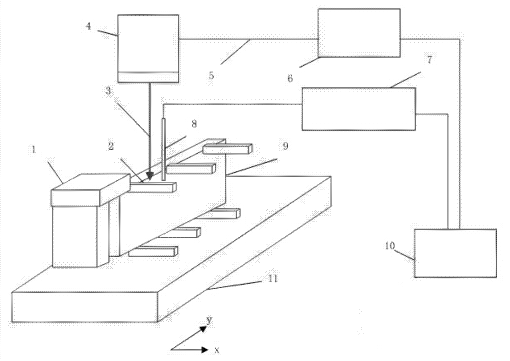
[0016] Such as figure 1 As shown, the chip lead shaping device based on laser thermal stress forming technology includes two parts: laser thermal stress shaping system and non-contact displacement measurement system.

[0017] The laser thermal stress shaping system includes a two-dimensional motion platform 11 , a chip holder 1 , a laser scanning unit 4 and a fiber laser 6 . The chip holder 1 is used to clamp the chip 9 , and both are arranged on the two-dimensional motion platform 11 , and the chip 9 has a plurality of chip pins 2 . The laser light emitted by the fiber laser 6 passes through the transmission fiber 5 and enters the laser scanning unit 4 for scanning movement. Finally, the focused laser 3 is projected on the chip pin 2 to be shaped, and the deformed chip pin 2 is shaped.

[0018] The non-contact displacement measurement system specifically i...


PUM


Abstract

Disclosed are a chip pin shaping device and method based on laser thermal stress shaping, and the device and method belong to the field of a semiconductor. To overcome a defect, which exists in the prior art, that the consistency precision of pins after correction is not easy to control, a chip is fixed on the chip pin shaping device through a chip clamp and a two-dimension motion platform is enabled to carry out scanning motion along a diagramed y axis. Through a sensor probe, relative height differences of chip pins are measured and obtained. Through a sensor controller, the measurement result is transmitted to a computer. The relative position of focusing laser on the chip pins is adjusted so that the scanning direction of the focusing laser is parallel with the direction of the diagrammed y axis. According to measured target shaping heights of the chip pins, the laser power and the scanning speed of an optical-fiber laser are sent through the computer and laser shaping processing is carried out on the pins. The relative heights of the pins are measured again through the sensor probe and then the computer decides through a corresponding program to continue shaping processing on a current pin or to carry out shaping on a next pin until all the pins meet tolerance demands.

Description

technical field [0001] The invention relates to a chip pin shaping device and method based on laser thermal stress forming technology, and belongs to the technical field of semiconductors. Background technique [0002] In the field of semiconductor manufacturing, dual in-line (DIP) packaged IC chips have been widely used due to the advantages of convenient installation and wiring, but due to the influence of vibration and impact in the manufacturing process and transportation and packaging links, the chip pins are often bent. Sometimes, integrated circuit manufacturers must detect chip pins and reject unqualified products before installing electronic components, which increases the manufacturing cost and production cycle of electronic products; on the other hand, as the replacement cycle of electronic products becomes more and more Fast, a large number of discarded DIP packaged IC chips are produced. Most of these chips can still be used, but the pins of the chips are bent d...

Claims


Application Information

Patent Timeline
Patent Type & Authority Applications(China)
IPC IPC(8): H01L21/67H01L21/48
CPCH01L21/4896H01L21/67092H01L2221/67
Inventor 王东平吴志会倪明阳李显凌杨怀江隋永新
Owner BEIJING GUOWANG OPTICAL TECH CO LTD
Why Eureka
Try Eureka