

Array substrate and preparation method thereof, display panel and display device
An array substrate and substrate substrate technology, which is applied in the fields of array substrate, its preparation, display panel and display device, can solve the problems of coating film layer ripple, affecting the yield rate of the array substrate, large hole depth and size, etc. The effect of reducing and avoiding the ripple of the coating film and improving the yield
- Summary
- Abstract
- Description
- Claims
- Application Information
AI Technical Summary
Problems solved by technology
Method used
Image


Examples
Embodiment 1
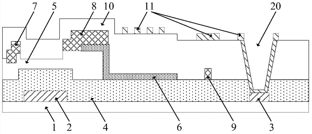
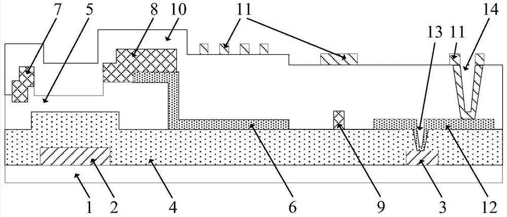
[0065] An embodiment of the present invention provides an array substrate, including a base substrate, a gate metal layer, a gate insulating layer, an active layer, a source-drain metal layer, a passivation layer, and a common electrode layer sequentially formed on the base substrate , and a pixel electrode layer located between the active layer and the source-drain metal layer or between the source-drain metal layer and the passivation layer; the gate metal layer includes a gate electrode and a common electrode line;
[0066] The pixel electrode layer or the source-drain metal layer includes a connection electrode, the connection electrode is electrically connected to the common electrode line through the first via hole on the gate insulating layer, and the connection electrode is connected to the common electrode line through the second via hole on the passivation layer. The common electrode is electrically connected.
[0067] In the embodiment of the present invention, by s...
Embodiment 2
[0096] An embodiment of the present invention provides a display panel, including the array substrate of the above embodiment. Of course, the display panel in this embodiment may also include a color filter substrate, liquid crystal, and other commonly used accessories, which will not be repeated here.
[0097] The beneficial effects of the embodiments of the present invention are as follows: the pixel electrode layer or the source-drain metal layer is provided with a connecting electrode, the connecting electrode is electrically connected to the common electrode line through the first via hole, and the common electrode is electrically connected to the connecting electrode through the second via hole, realizing For the electrical connection between the common electrode and the common electrode line, since the first via hole and the second via hole are respectively arranged on different layers and are electrically connected through the connecting electrode, the depth and size of...
Embodiment 3
[0099] An embodiment of the present invention provides a display device, including the display panel of the above embodiment. The display device of the embodiment may further include a backlight module, a frame, a base, etc., which will not be repeated here.
[0100] The beneficial effects of the embodiments of the present invention are as follows: a connection electrode is provided between the gate insulating layer and the passivation layer of the array substrate, the connection electrode is electrically connected to the common electrode line through the first via hole, and the common electrode is connected to the connection electrode through the second via hole Electrical connection to realize the electrical connection between the common electrode and the common electrode line. Since the first via hole and the second via hole are respectively arranged in different layers and realize electrical connection through the connecting electrode, the depth and size of the hole are com...
PUM
 Abstract
Description
Claims
Application Information