Atomic layer deposition equipment

A technology of atomic layer deposition and equipment, applied in the direction of coating, metal material coating process, gaseous chemical plating, etc., can solve the problems of long time consumption, slow atomic layer deposition rate, and difficulty in meeting large-scale production, and achieve The effect of increasing productivity and improving process efficiency

Active Publication Date: 2015-02-11
BEIJING NAURA MICROELECTRONICS EQUIP CO LTD
View PDF6 Cites 171 Cited by
  • Summary
  • Abstract
  • Description
  • Claims
  • Application Information

AI Technical Summary

Problems solved by technology

[0006] First, the deposition rate of atomic layers is slow due to the self-inhibiting nature of the reaction between the gases from the two sources (i.e., the two cannot continue to react) and it takes a significant amount of time to complete all of the above process steps , For example, it takes at least 300-400s to deposit an aluminum oxide film with a thickness of 20nm, which makes the productivity of atomic layer deposition equipment very low, and it is difficult to meet the needs of large-scale production
[0007] Its two, before carrying out step 4, that is, before passing into the next gas in the reaction chamber 10, all need to carry out the step of removing the gas remaining in the reaction chamber 10 by means of a purge gas, which makes the whole process complete A large portion of the process time is consumed in this step, which further reduces the throughput of the ALD tool

Method used


Image

  • Atomic layer deposition equipment
  • Atomic layer deposition equipment
  • Atomic layer deposition equipment

Examples


Embodiment Construction

[0035] In order to enable those skilled in the art to better understand the technical solutions of the present invention, the atomic layer deposition equipment provided by the present invention will be described in detail below with reference to the accompanying drawings.

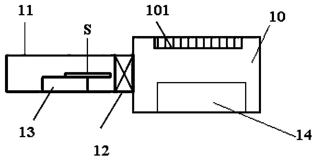
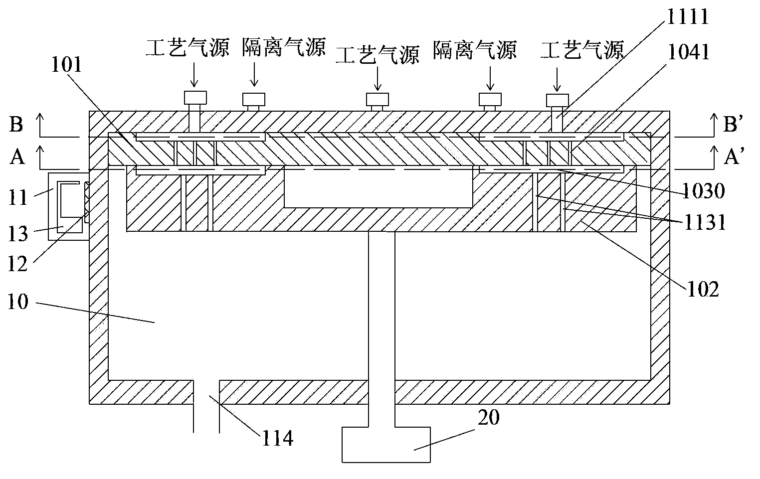
[0036] Figure 3A It is a cross-sectional view of the atomic layer deposition equipment provided by the first embodiment of the present invention. Figure 3B for Figure 3A A cross-sectional view along the line A-A'. Figure 3C for Figure 3A Top view of the gas distribution plate. Figure 3D for Figure 3A Top view of the base plate. Figure 3E for Figure 3A A cross-sectional view along the line B-B'. Please also refer to Figure 3A , Figure 3B , Figure 3C , Figure 3D and Figure 3E , the atomic layer deposition equipment includes a reaction chamber 10, a loading and unloading chamber 11, a gate valve 12 and a gas source. Wherein, the reaction chamber includes a gas distribution plate 101,...


PUM


Abstract

Provided atomic layer deposition equipment comprises a reaction chamber and a gas source; the reaction chamber is inside provided with a gas distribution plate arranged at the top, a base disc and a rotary driving mechanism; the upper surface of the base disc and the lower surface of the gas distribution plate are mutually superposed; multiple sub-spaces uniformly distributed along the circumferential direction of the reaction chamber at intervals are formed between the upper surface of the base disc and the lower surface of the gas distribution plate, the multiple sub-spaces are successively arranged according to the operation sequence, and each sub-space is corresponding to one operation in a process of performing once technology on a base chip; and the rotary driving mechanism is used to drive the base disc to rotate relatively to the gas distribution plate so as to enable the base disc to drive all base chips thereon to be successively placed into the multiple sub-spaces for technological processing according to the operation sequence. The provided atomic deposition equipment is capable of processing multiple base chips at the same time by using different operations, thereby improving the technological efficiency and further improving the production power.

Description

technical field [0001] The invention belongs to the technical field of microelectronic processing, and in particular relates to an atomic layer deposition device. Background technique [0002] In the field of microelectronics processing technology, atomic layer deposition (ALD) is a device that deposits substances layer by layer on the surface of a substrate in the form of a single atomic film. Due to the diversity of deposition materials and the accuracy of deposition thickness, it has been more and more widely used. [0003] figure 1 It is a schematic structural diagram of an existing atomic layer deposition equipment. figure 2 A flow chart of the atomic layer deposition process. Please also refer to figure 1 and figure 2 , the atomic layer deposition apparatus includes a loading and unloading chamber 11 and a reaction chamber 10 arranged in parallel, and a gate valve 12 arranged between the two and used for communicating or isolating the two. Wherein, a gas distri...

Claims


Application Information

Patent Timeline
Patent Type & Authority Applications(China)
IPC IPC(8): C23C16/455
CPCC23C16/455
Inventor 南建辉宋巧丽李强王宝全苏晓峰
Owner BEIJING NAURA MICROELECTRONICS EQUIP CO LTD
Why Eureka
Try Eureka