An active single-ended probe and a test and measurement instrument
A single-source, amplifier technology, applied in the field of test and measurement instruments and active single-ended probes, to achieve the effects of ensuring in-band flatness parameters, reducing interference, and good symmetry
- Summary
- Abstract
- Description
- Claims
- Application Information
AI Technical Summary
Problems solved by technology
Method used
Image
Examples
Embodiment 1
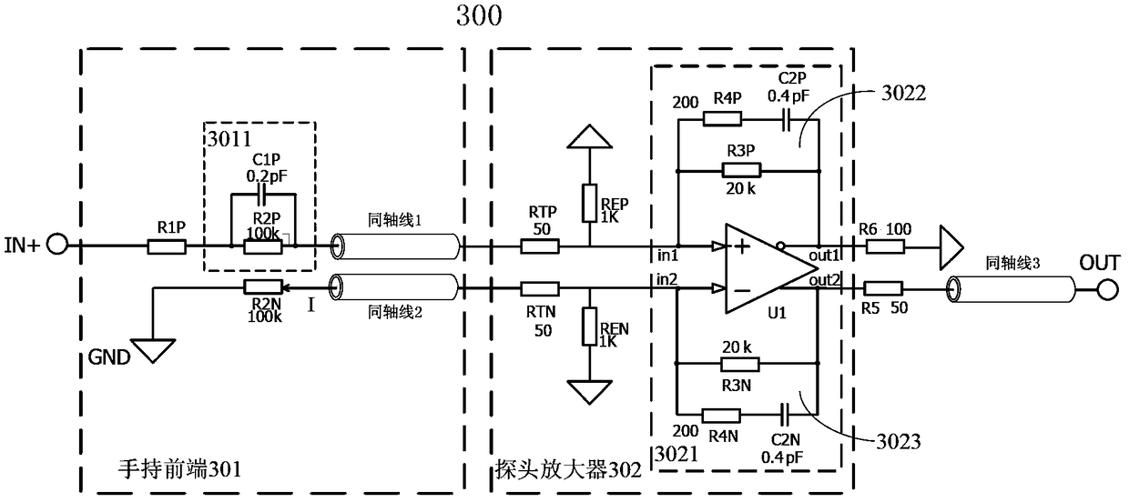
[0047] refer to image 3 , shows a circuit diagram of an active single-ended probe 300 provided in Embodiment 1 of the present invention. The active single-ended probe 300 includes: a signal input terminal IN+, a hand-held front end 301 , a probe amplifier 302 and a signal output terminal OUT.
[0048] The handheld front end 301 (also called the handle end) includes: a first resistor R1P, an input impedance unit 3011 and a second resistor R2N; one end of the first resistor R1P is connected to the signal input terminal IN+, and the other end is connected to the input terminal of the input impedance unit 3011. One end of the second resistor R2N is grounded to GND;
[0049] The probe amplifier 302 includes: a first terminal resistor RTP, a second terminal resistor RTN and an amplifier unit 3021; one end of the first terminal resistor RTP is electrically connected to the output end of the impedance unit 3011, and the other end is connected to the first input terminal in1 of the...
Embodiment 2
[0057] refer to Figure 4 , shows a circuit diagram of an active single-ended probe 400 provided in Embodiment 2 of the present invention. The active single-ended probe 400 includes: a signal input terminal IN+, a hand-held front end 401 , a probe amplifier 402 and a signal output terminal OUT. The handheld front end 401 includes: a first resistor R1P, an input impedance unit 4011 and a second resistor R2N; the probe amplifier 402 includes: a first terminal resistor RTP, a second terminal resistor RTN and an amplifier unit 4021 . For the connection relationship of each component, the internal circuit structure, and the value range of each component, please refer to Embodiment 1.
[0058] The difference from Embodiment 1 is that one end of the first balancing resistor REP is grounded, the non-grounding end of the first balancing resistor REP is connected to the output end of the input impedance unit 4011, one end of the second balancing resistor REN is grounded, and the second...
Embodiment 3
[0060] refer to Figure 5 , shows a circuit diagram of an active single-ended probe 500 provided in Embodiment 3 of the present invention. The active single-ended probe 500 includes: a signal input terminal IN+, a hand-held front end 501 , a probe amplifier 502 and a signal output terminal OUT. The handheld front end 501 includes: a first resistor R1P, an input impedance unit 5011 and a second resistor R2N; the probe amplifier 502 includes: a first terminal resistor RTP, a second terminal resistor RTN and an amplifier unit 5021 . For the connection relationship of each component, the internal circuit structure, and the value range of each component, please refer to Embodiment 1.
[0061]The difference from Embodiment 1 is that one end of the first balancing resistor REP is grounded, and the non-grounding end of the first balancing resistor REP is connected to the series connection between the coaxial line 1 and the first terminal resistor RTP, that is, the coaxial line 1 out...
PUM
 Abstract
Description
Claims
Application Information


