Multilayer ceramic electronic part, board having the same mounted thereon, and manufacturing method thereof

A technology of electronic components and multilayer ceramics, which is applied in the direction of printed circuit manufacturing, printed circuit components, fixed capacitor components, etc., can solve problems such as discomfort for the listener, and achieve the effect of reducing acoustic noise

Inactive Publication Date: 2015-02-11
SAMSUNG ELECTRO MECHANICS CO LTD
View PDF1 Cites 15 Cited by
  • Summary
  • Abstract
  • Description
  • Claims
  • Application Information

AI Technical Summary

Problems solved by technology

[0007] The vibrating sound may have a frequency corresponding to audio in the range of 20Hz to 20000Hz, which causes discomfort to the listener

Method used


Image

  • Multilayer ceramic electronic part, board having the same mounted thereon, and manufacturing method thereof
  • Multilayer ceramic electronic part, board having the same mounted thereon, and manufacturing method thereof
  • Multilayer ceramic electronic part, board having the same mounted thereon, and manufacturing method thereof

Examples


Embodiment Construction

[0028] Exemplary embodiments of the present disclosure will now be described in detail with reference to the accompanying drawings.

[0029] This disclosure, however, may be embodied in many different forms and should not be construed as limited to the specific embodiments set forth herein. Rather, these embodiments are provided so that this disclosure will be thorough and complete, and will fully convey the scope of the disclosure to those skilled in the art.

[0030] In the drawings, the shapes and dimensions of elements may be exaggerated for clarity, and the same reference numerals will be used throughout to designate the same or like elements.

[0031] Hereinafter, a multilayer ceramic electronic component such as a multilayer ceramic capacitor according to an exemplary embodiment of the present disclosure will be described, but the present disclosure is not limited thereto.

[0032] Multilayer Ceramic Capacitors

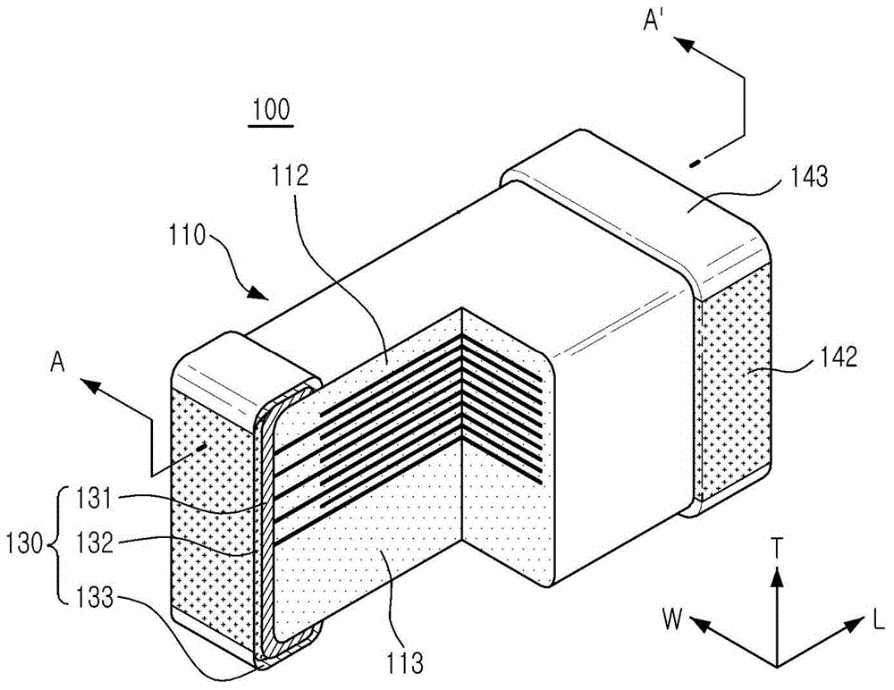
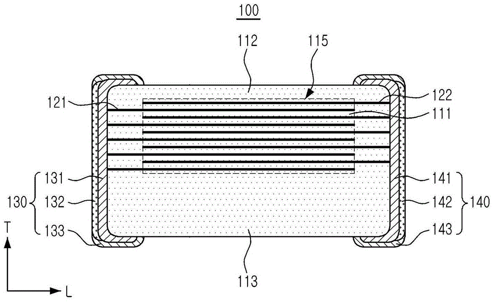
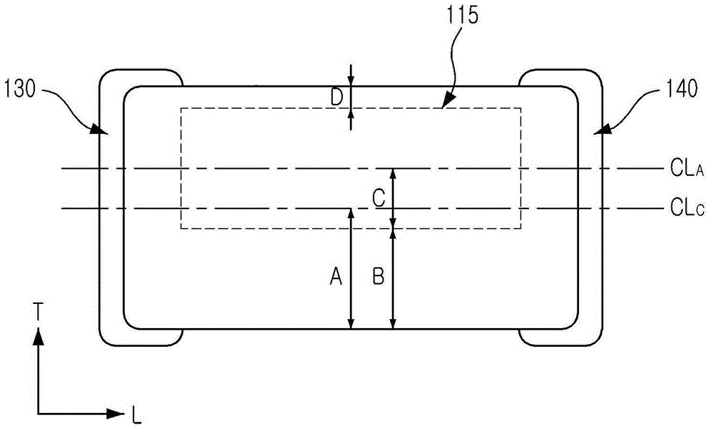
[0033] figure 1 is a partially cutaway perspective v...


PUM

PropertyMeasurementUnit
thicknessaaaaaaaaaa
thicknessaaaaaaaaaa

Abstract

A multilayer ceramic electronic part may include: a ceramic body; an active layer including a plurality of first and second internal electrodes disposed to be alternately exposed to both end surfaces of the ceramic body, having the dielectric layer therebetween; an upper cover layer formed on an upper portion of the active layer; a lower cover layer formed on a lower portion of the active layer and having a thickness thicker than that of the upper cover layer; and first and second external electrodes electrically connected to the first and second internal electrodes, wherein the first and second external electrodes include: first and second conductive layers extended from both end surfaces of the ceramic body onto upper and lower main surfaces thereof; and first and second insulation layers formed on the first and second conductive layers disposed on both end surfaces of the ceramic body.

Description

[0001] This application claims the benefit of Korean Patent Application No. 10-2013-0094838 filed with the Korean Intellectual Property Office on Aug. 9, 2013, the disclosure of which is hereby incorporated by reference. technical field [0002] The present disclosure relates to a multilayer ceramic electronic component, a board on which the multilayer ceramic electronic component is mounted, and a manufacturing method thereof. Background technique [0003] According to the recent trend of miniaturization of electronic products, multilayer ceramic electronic parts of small size and high capacitance have been used therein. [0004] Therefore, many efforts have been made in making dielectric layers and internal electrodes thinner and stacked in increasing numbers using various methods. Recently, multilayer ceramic electronic components have been manufactured in which the thickness of the dielectric layer is relatively low and the number of stacked layers is increased. [0005...

Claims


Application Information

Patent Timeline
Patent Type & Authority Applications(China)
IPC IPC(8): H01G4/30H01G4/232H05K1/18
CPCH05K1/0213H05K3/384H01G4/30H05K3/4629H01G4/12H01G2/06H01G4/232
Inventor 朴祥秀安永圭金斗永
Owner SAMSUNG ELECTRO MECHANICS CO LTD
Why Eureka
Try Eureka