Supercharge Your Innovation With Domain-Expert AI Agents!

Display panel and manufacturing method thereof

A manufacturing method and display panel technology, applied in semiconductor/solid-state device manufacturing, optics, instruments, etc., can solve the problems of increasing process cost and difficulty of process, and achieve the effect of improving quality

Inactive Publication Date: 2015-02-11
HONG FU JIN PRECISION IND (SHENZHEN) CO LTD +1
View PDF5 Cites 4 Cited by
  • Summary
  • Abstract
  • Description
  • Claims
  • Application Information

AI Technical Summary

Problems solved by technology

However, forming the etching barrier layer requires an additional photomask and precise alignment between the photomask and the channel layer, which will increase the difficulty of the process and increase the cost of the process

Method used


Image

  • Display panel and manufacturing method thereof
  • Display panel and manufacturing method thereof
  • Display panel and manufacturing method thereof

Examples


Embodiment Construction

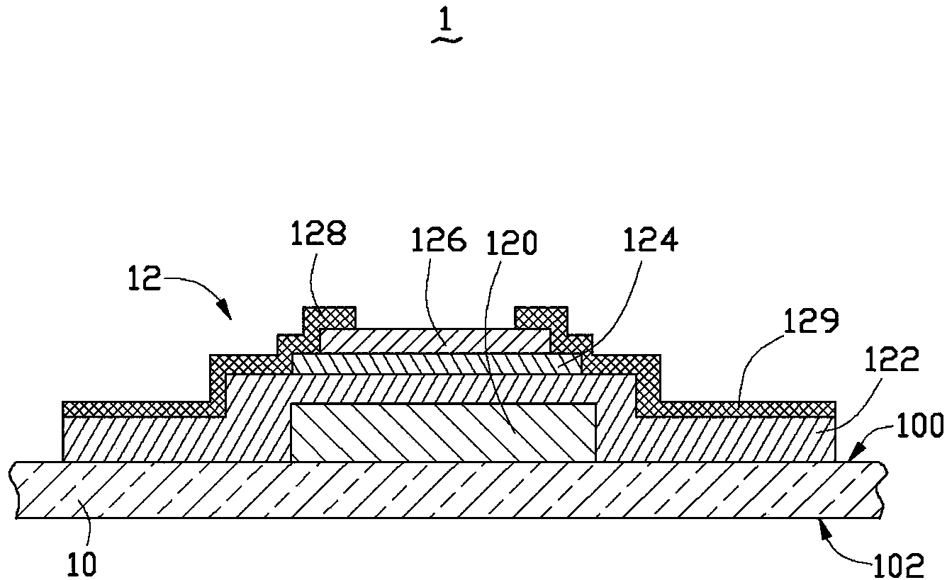
[0025] Such as figure 1 As shown, the display panel 1 provided by the embodiment of the present invention includes a substrate 10 and a plurality of thin film transistors 12 (Thin Film Transistor, TFT) disposed on the substrate 10 and arranged in an array. The TFT 12 includes a gate 120 , a gate insulating layer 122 , a semiconductor pattern 124 , an etch stop pattern 126 , a source 128 and a drain 129 . The gate 120 is disposed on the substrate 10 and extends along a first direction A. Referring to FIG. The gate insulating layer 122 covers the gate 120 . The semiconductor pattern 124 is disposed on the gate insulating layer 122 . The etch stop pattern 126 covers the channel region of the semiconductor pattern 124 to prevent the etchant from damaging the channel region of the semiconductor pattern 124 during the fabrication of the display panel 1 . The source 128 and the drain 129 are respectively disposed on opposite sides symmetrical to the gate 120 and partly cover the e...


PUM


Abstract

A display panel manufacturing method includes forming a gate electrode on a substrate and a gate insulator, a semiconductor layer, and an etch stop layer covering the gate electrode. A photoresist layer covering on the etch stop layer is pattern from two opposite side of the substrate by two photolithography processes to form a photoresist pattern. The etch stop layer is dry etched to form an etch stop pattern via the photoresist pattern. The photoresist pattern is formed again by two photolithography processes. The semiconductor layer is wet etched to form a semiconductor pattern via the photoresist pattern. A source electrode and a drain electrode is formed corresponding to two opposite sides of the gate electrode to orderly cover the etch pattern, the semiconductor pattern, and the gate insulator.

Description

technical field [0001] The invention relates to a manufacturing method of a display panel. Background technique [0002] In order to prevent the channel layer of the TFT (Thin Film Transistor, TFT) from being etched during the manufacturing process of the existing liquid crystal display panel, an etch stop layer is usually formed on the channel layer. However, forming the etching barrier layer requires an additional photomask and precisely aligning the photomask with the channel layer, which increases the difficulty of the process and increases the cost of the process. Contents of the invention [0003] In view of this, it is necessary to provide a method for manufacturing a display panel without adding an additional photomask to form an etching stopper layer. [0004] A method for manufacturing a display panel, comprising the steps of: [0005] A substrate is provided, and the substrate includes a first surface and a second surface sequentially arranged in parallel alon...

Claims


Application Information

Patent Timeline
Patent Type & Authority Applications(China)
IPC IPC(8): H01L21/77G02F1/1333
CPCH01L27/127H01L27/1225H01L29/7869H01L29/66969
Inventor 施博理
Owner HONG FU JIN PRECISION IND (SHENZHEN) CO LTD
Features
  • R&D
  • Intellectual Property
  • Life Sciences
  • Materials
  • Tech Scout
  • Unparalleled Data Quality
  • Higher Quality Content
  • 60% Fewer Hallucinations
Learn More