
image sensing module

A technology of image sensing and bumps, which is applied in the direction of image communication, TV, color TV parts, etc., can solve the problems affecting the image quality, etc., and achieve the effect of improving image quality and reducing the impact

Active Publication Date: 2018-07-24
GUANGZHOU LUXVISIONS INNOVATION TECH LTD
View PDF5 Cites 0 Cited by
  • Summary
  • Abstract
  • Description
  • Claims
  • Application Information

AI Technical Summary

Problems solved by technology

Although the degree of deformation may not be observable by human eyes, when the chip module and the lens module are assembled on the circuit board, it is easy to make the optical axis of the lens module deviate from the optical axis of the chip module, which affects the final imaging quality

Method used


Image

  • image sensing module
  • image sensing module
  • image sensing module

Examples


Embodiment Construction

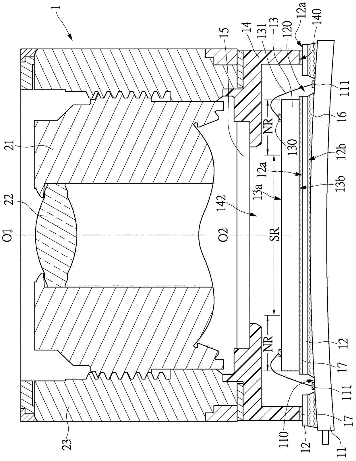
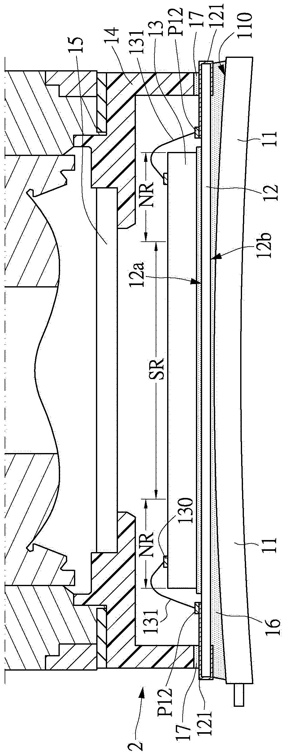
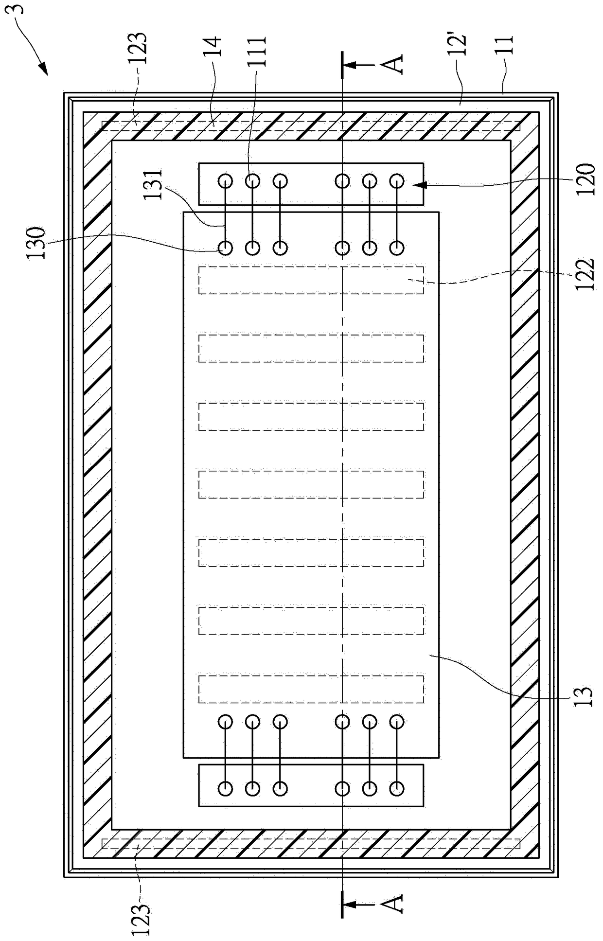
[0049] Please refer to figure 1 , shows a schematic cross-sectional view of an image acquisition device according to an embodiment of the present invention. The image sensing module 1 includes a circuit board 11 , a base material 12 , an image sensing chip 13 , a support base 14 , a cover plate 15 , a lens barrel 21 , a lens group 22 and a lens frame 23 .

[0050] The circuit board 11 has circuit structures such as external circuits (not shown), assembly surface 110 and internal circuits (not shown). The external circuit is disposed on the assembly surface 110 of the circuit board 11 and includes a plurality of contact pads 111 and a plurality of wires (not shown). The material of the circuit board can be an organic substrate, such as epoxy resin type FR5 or FR4, bismaleimide-triazine (BismaleimideTriazine, BT) resin. In addition, glass, ceramics and silicon can also be used as the material of the circuit board 11 . Since the various materials used to make the circuit board...


PUM


Abstract

Provided is an image sensing module which comprises a circuit board, mat material, an image sensing chip, a supporting base and a cover plate. The mat material is arranged on the assembling surface of the circuit board, and the mat material is provided with a bearing surface and a lower surface which is opposite to the bearing surface. The image sensing chip is arranged on the bearing surface and is provided with a bottom surface, wherein the bottom surface faces the bearing surface in arrangement. The supporting base is arranged on the mat material, wherein the bottom part of the support base is provided with a bottom plane facing the bearing surface. The bearing face is used for enabling the bottom plane and the bottom surface to be parallel. The cover plate is arranged on the supporting base.

Description

technical field [0001] The invention relates to an image sensing module improved for images. Background technique [0002] An image sensing module (for example: a digital camera) converts the image captured by the lens into a digital image signal through a chip module, and then stores the digital image signal in a storage medium. The chip module and the carrier for carrying the lens module are usually arranged on a circuit board. Ideally, the optical axis of the lens module should be aligned with the optical axis of the sensing area of ​​the chip module. [0003] However, circuit boards are composite materials. When the heat treatment process is applied to the circuit board, since the thermal expansion coefficients of the various materials of the circuit board are different, it is easy to cause the circuit board as a whole to warp. That is to say, before the chip module and the lens module are arranged, the surface of the circuit board is not a flat surface, but may be a ...

Claims


Application Information

Patent Timeline
Patent Type & Authority Patents(China)
IPC IPC(8): H04N5/357H04N5/3745H04N5/378
Inventor 詹欣达
Owner GUANGZHOU LUXVISIONS INNOVATION TECH LTD
Learn More