A method for preparing copper indium gallium selenide thin films based on photochemical deposition

A photochemical deposition, copper indium gallium selenide technology, applied in the field of optoelectronic materials and new energy, can solve the problem of low cost and achieve the effect of low equipment requirements, good shape and compact structure

Active Publication Date: 2016-08-24
CENT SOUTH UNIV
View PDF3 Cites 0 Cited by
  • Summary
  • Abstract
  • Description
  • Claims
  • Application Information

AI Technical Summary

Problems solved by technology

[0005] In view of the defects in the preparation method of copper indium gallium selenide (CIGS) thin film materials in the prior art, the present invention applies photochemical deposition to the preparation process of copper indium gallium selenide thin film for the first time, and overcomes the defects of traditional photochemical methods. The purpose is to It is to propose a method for preparing copper indium gallium selenide thin film with good surface morphology, high density and controllable composition. This method has high raw material utilization rate and low cost, and can be popularized and produced on a large scale

Method used


Image

  • A method for preparing copper indium gallium selenide thin films based on photochemical deposition
  • A method for preparing copper indium gallium selenide thin films based on photochemical deposition
  • A method for preparing copper indium gallium selenide thin films based on photochemical deposition

Examples


Embodiment 1

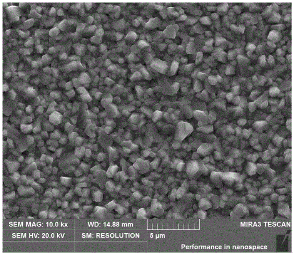
[0037] Se was plated on the Mo glass substrate with a thickness of 700nm by laser pulse deposition process. The solute composition of the reaction solution is 0.02mol / L CuCl 2 , 0.01mol / L InCl 3 , 0.01mol / L SeO 2 , 0.01mol / L GaCl 3 , 0.75mol / L K 2 S 2 o 3 , adjust the pH to 7.0 with dilute hydrochloric acid or sodium hydroxide; adopt the following photochemical deposition parameters: the incident light is a monochromatic light source of 400nm (the light intensity is 150mW / cm 2 ), the solution temperature was 40°C, and the deposition time was 90 minutes. Copper indium gallium selenide thin film Cu is deposited on the surface of the substrate with a thickness of 1-2 μm a In b Ga c Se d , and finally the film was placed in Se-containing argon, and heat-treated at a temperature of 580° C. for 40 minutes. image 3 It is the XRD pattern before and after the annealing of the copper indium gallium selenium thin film prepared in embodiment 3.

[0038] From image 3 It can ...

Embodiment 2

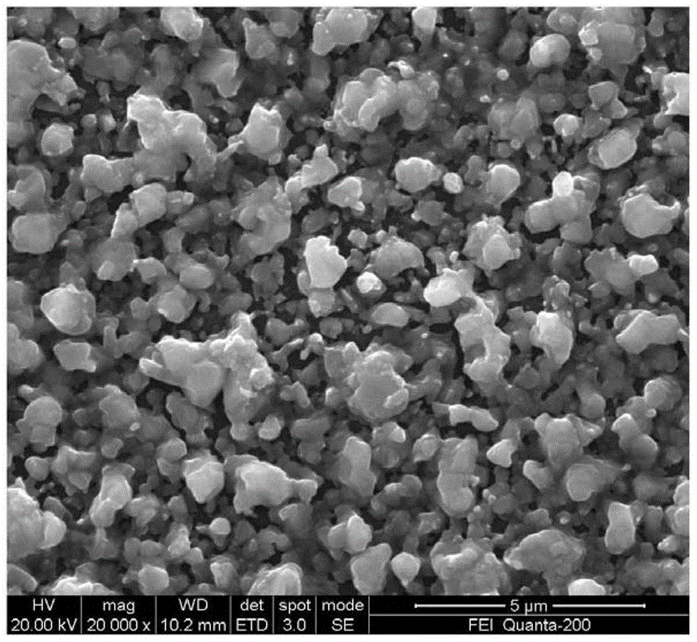
[0039] S was plated on Mo glass substrate with a thickness of 900nm by laser pulse deposition process. The solute composition of the reaction solution is 0.05mol / L CuSO 4 , 0.1mol / L SeO 2 , 1.5mol / L K 2 S 2 o 3 , 1mol / L K 2 SO 3 , adjust the pH to 4 with dilute hydrochloric acid or sodium hydroxide; adopt the following photochemical deposition parameters: the incident light is a monochromatic light source of 300nm (the light intensity is 300mW / cm 2 ), the solution temperature was 50°C, and the deposition time was 100 minutes. Deposit a 3-4 μm thick copper indium gallium selenide thin film Cu on the surface of the substrate a In b Ga c Se d , and finally the film was placed in Se-containing nitrogen and heat-treated at 450° C. for 60 minutes. The surface of the prepared film is smooth and dense, without cracks and holes, and the grain size is also significantly improved.

Embodiment 3

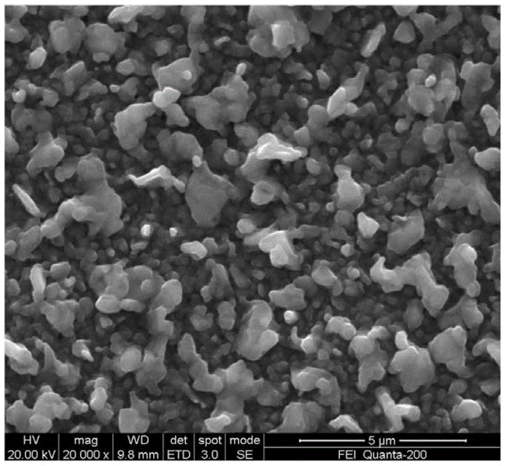
[0041] Se was plated on Mo glass substrate with a thickness of 800nm ​​by magnetron sputtering process. First, the solute composition is 0.02mol / L CuCl 2 , 0.01mol / L InCl 3 , 0.01mol / L SeO 2 , 0.75mol / L Li 2 S 2 o 3 , adjust the pH to 6 with dilute hydrochloric acid or sodium hydroxide; adopt the following photochemical deposition parameters: the incident light is a monochromatic light source of 700nm (the light intensity is 300mW / cm 2 ), the solution temperature was 80°C, and the deposition time was 20 minutes. Deposit a 0.5 μm thick CuInGaSe thin film Cu on the substrate surface a In b Ga c Se d , and finally the film was placed in Se-containing nitrogen and heat-treated at a temperature of 500° C. for 0.6 hours. The surface of the prepared film is smooth and dense, without cracks and holes, and the grain size is also significantly improved.


PUM

PropertyMeasurementUnit
wavelengthaaaaaaaaaa
thicknessaaaaaaaaaa
thicknessaaaaaaaaaa

Abstract

The invention discloses a method for preparing a CIGS film based on photochemistry deposition. According to the method, a conductive substrate is plated with a Se or S film firstly, then the conductive substrate plated with the Se or S film is placed in a solution system containing at least two kinds of indium ions, gallium ions, selenium ions and copper ions and a photoelectron releasing agent for photochemistry deposition, and then the CIGS film is obtained. According to the method, the photochemistry deposition method is successfully applied to the preparation of the CIGS film, the growth situation and morphology of the photochemistry deposition CIGS film can be effectively controlled, the prepared CIGS film is good in surface morphology and high in density, composition is controllable, the problems of poor deposition controllability and film nonuniformity existing in a traditional photochemistry deposition process are effectively solved, the material utilization rate is high, cost is low, and large-scale production and promotion can be achieved.

Description

technical field [0001] The invention relates to a method for preparing a copper indium gallium selenium thin film based on photochemical deposition, which belongs to the technical field of photoelectric materials and new energy sources. Background technique [0002] CuInSe 2 (CIS) thin film solar cells have become one of the most important and most promising solar cells. CuInSe 2 The thin film is a direct energy gap semiconductor material with an energy gap of 1.05eV, and can be formed by doping Ga to form copper indium gallium selenide Cu(In,Ga)Se 2 (CIGS) continuously adjusts the energy gap width within 1.05-1.67eV, which is suitable for the photoelectric conversion requirements of sunlight; copper indium gallium selenide (CIGS) thin film has a high light absorption coefficient (up to 10 5 cm -1 ), and stable performance, no light attenuation effect, so it has been widely concerned by the photovoltaic industry. [0003] There are vacuum and non-vacuum preparation meth...

Claims


Application Information

Patent Timeline
Patent Type & Authority Patents(China)
IPC IPC(8): H01L31/18C23C14/06
CPCC23C14/06H01L31/18Y02P70/50
Inventor 李劼秦勤刘芳洋赖延清杨佳赵联波张坤王庆龙
Owner CENT SOUTH UNIV
Why Eureka
Try Eureka