

Touch display panel and touch display device
A touch display panel, color filter substrate technology, applied in optics, instruments, electrical digital data processing and other directions, can solve the problems of reduced sensitivity, interference of liquid crystal deflection, large load of touch display panel, etc., to reduce load, reduce power consumption, The effect of increasing sensitivity
- Summary
- Abstract
- Description
- Claims
- Application Information
AI Technical Summary
Problems solved by technology
Method used
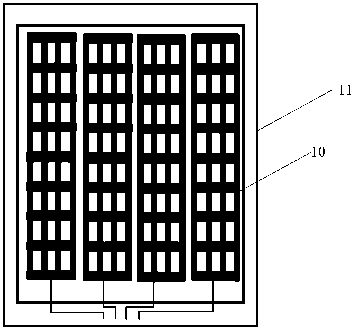
Image

Examples
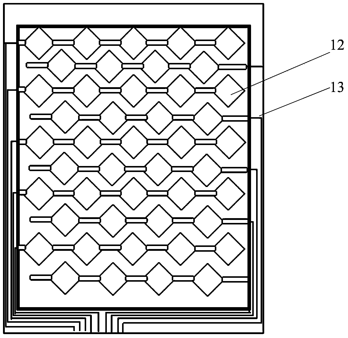
Embodiment 1
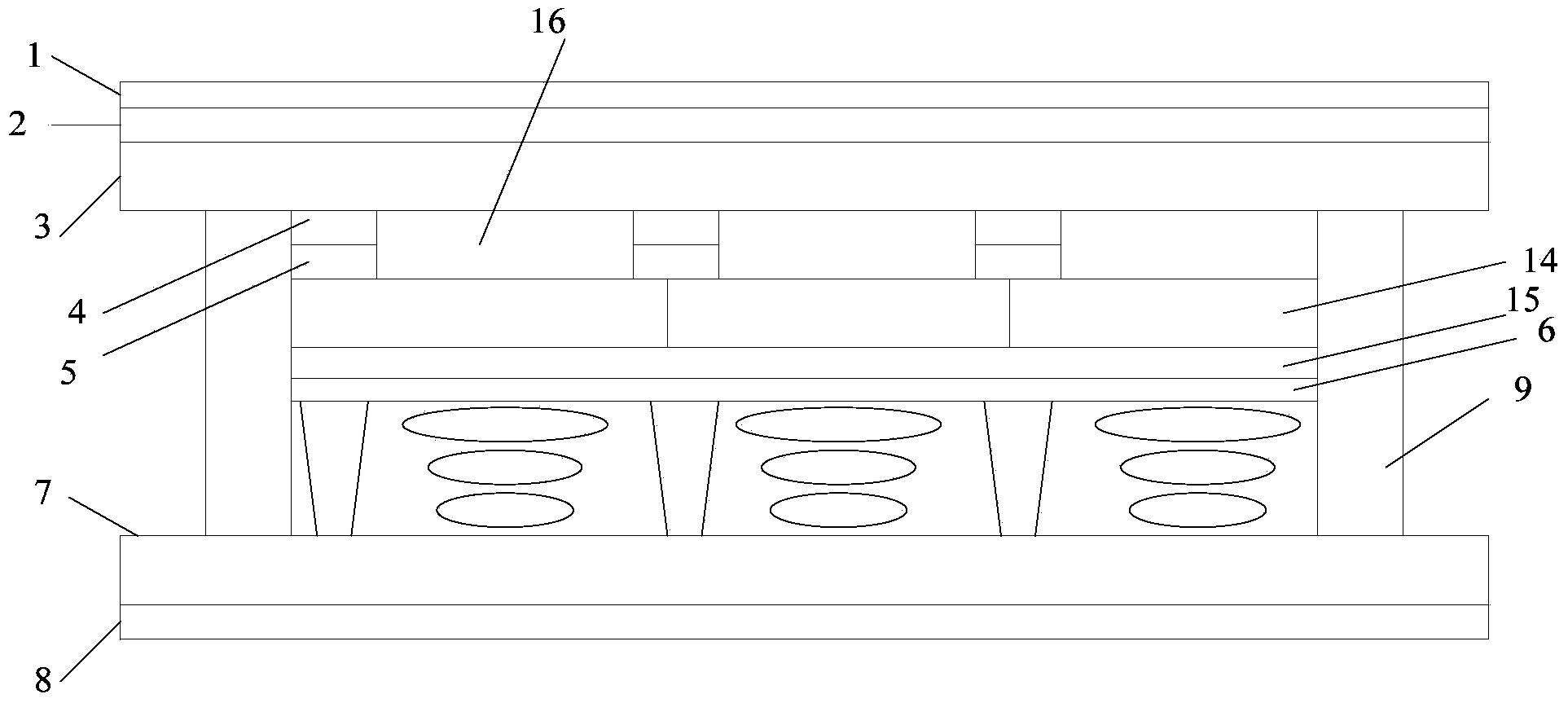
[0064] In the prior art, a transparent conductive layer is used to fabricate the emitter electrode inside the color filter substrate, so that the touch signal may interfere with the deflection of the liquid crystal and affect the display effect of the touch display panel. In addition, the signal on the thin film transistor will also interfere with the touch signal, reducing the sensitivity of the touch display panel; and for the display panel that uses the common signal electrode to make the emitter electrode, there is a problem of time-division multiplexing of the common electrode signal and the touch signal. As a result, the scanning time of the common electrode signal and the touch signal is insufficient, and the large size and high PPI (number of pixels) of the product cannot be realized. At the same time, due to the high resistivity of the transparent conductive layer, the use of the transparent conductive layer to make the transmitting electrode and the receiving electrod...
Embodiment 2
[0074] In the prior art, a transparent conductive layer is used to fabricate the emitter electrode inside the color filter substrate, so that the touch signal may interfere with the deflection of the liquid crystal and affect the display effect of the touch display panel. In addition, the signal on the thin film transistor will also interfere with the touch signal, reducing the sensitivity of the touch display panel; and for the display panel that uses the common signal electrode to make the emitter electrode, there is a problem of time-division multiplexing of the common electrode signal and the touch signal. As a result, the scanning time of the common electrode signal and the touch signal is insufficient, and the large size and high PPI of the product cannot be realized. At the same time, due to the high resistivity of the transparent conductive layer, the use of the transparent conductive layer to make the transmitting electrode and the receiving electrode will make the tou...
PUM
 Abstract
Description
Claims
Application Information