A Piezoelectric Modulated Vertical Cavity Semiconductor Laser Structure

A vertical cavity and semiconductor technology, applied in the direction of semiconductor lasers, lasers, devices for controlling output parameters of lasers, etc., can solve the problem of single modulation mode

Inactive Publication Date: 2018-01-09
BEIJING UNIV OF TECH
View PDF5 Cites 0 Cited by
  • Summary
  • Abstract
  • Description
  • Claims
  • Application Information

AI Technical Summary

Problems solved by technology

[0002] At present, the modulation of the output power of the vertical cavity semiconductor laser is mainly realized by changing the applied current, and the modulation method is single

Method used


Image

  • A Piezoelectric Modulated Vertical Cavity Semiconductor Laser Structure

Examples


Embodiment Construction

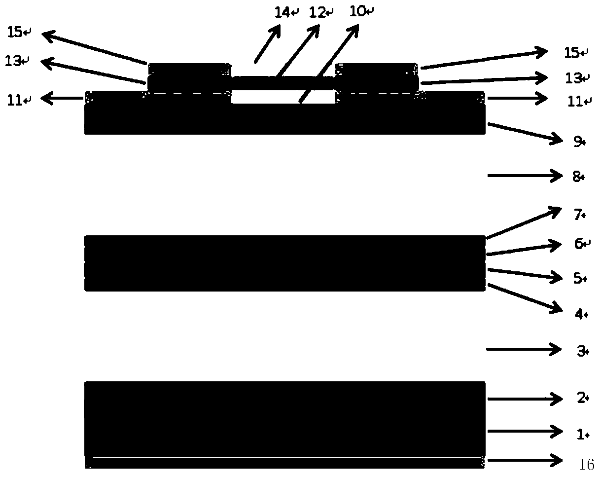
[0052] The structure of the piezoelectric modulation vertical cavity semiconductor laser used in the present invention is: the MOCVD (metal organic chemical vapor deposition) epitaxial growth method is adopted. Such as figure 1 Shown:

[0053]In n-GaAs(100)(Si:2x10) with a width of 250um 18 / cm 2 ) grow n-GaAs (Si: 2x10 18 / cm 2 ) buffer layer 2;

[0054] In n-GaAs (Si:2x10 18 / cm 2 ) on the buffer layer 2 grows 20 pairs of λ / 4 periodically repeated Al 0.9 Ga 0.1 As(81.7nm) / GaAs(69.6nm)(Si:2x10 18 / cm 2 ), forming an n-type DBR reflector 3;

[0055] Growth of n-Al with a thickness of 72.3 nm on the n-type mirror 3 0.2 Ga 0.8 As(Si:1×10 18 / cm 3 ) lower carrier confinement layer 4;

[0056] Gain region 5 with 3 quantum wells is grown on carrier lower confinement layer 4 (well material is In 0.2 Ga 0.8 As thickness is 8nm, barrier material is GaAs thickness is 10nm);

[0057] Growth of p-Al with a thickness of 72.3nm on the gain region 5 0.2 Ga 0.8 As(C:1×10...


PUM


Abstract

The invention provides a piezoelectric modulation vertical cavity semiconductor laser structure, which comprises: a single wafer substrate (1), a buffer layer (2), an n-type DBR mirror (3), a lower carrier confinement layer (4), Gain region (5), upper carrier confinement layer (6), photoelectric confinement layer (7), p-type DBR mirror (8), ohmic electrode contact layer (9), first transparent electrode (10), two The second gold layer (11), SiO2 anti-reflection film (12), two SiN insulating layers (13), the second transparent electrode (14), two third gold layers (15), the first gold layer (16) . It uses the piezoelectric properties of the SiO2 anti-reflection film to deform the cavity of the vertical cavity semiconductor laser to different degrees when it is powered on, so as to realize the piezoelectric modulation of the output power of the vertical cavity semiconductor laser.

Description

technical field [0001] The invention relates to the technical field of semiconductor laser devices, in particular to a piezoelectric modulation vertical cavity semiconductor laser structure. Background technique [0002] At present, the modulation of the output power of the vertical cavity semiconductor laser is mainly realized by changing the applied current, and the modulation method is single. Usually, the output end facet of the vertical cavity semiconductor laser needs to be plated with SiO 2 Anti-reflection coating to improve the micromolecular efficiency and enhance the light transmittance, while SiO 2 It is a material with piezoelectric properties. Therefore, the anti-reflection coating SiO can be used 2 The piezoelectric characteristics of the laser make the cavity of the laser change from a planar stable cavity to a non-planar unstable cavity, thereby realizing the modulation of the output power of the vertical cavity semiconductor laser. [0003] Piezoelectric...

Claims


Application Information

Patent Timeline
Patent Type & Authority Patents(China)
IPC IPC(8): H01S5/183H01S5/06H01S5/10
Inventor 王智勇吕朝蕙李军尧舜邱运涛贾冠男高祥宇雷宇鑫
Owner BEIJING UNIV OF TECH
Why Eureka
Try Eureka