Non-volatile semiconductor storage device

A storage device, non-volatile technology, applied in semiconductor devices, information storage, read-only memory, etc., can solve the problem that data cannot be written

Active Publication Date: 2015-02-25
FLOADIA
View PDF5 Cites 8 Cited by
  • Summary
  • Abstract
  • Description
  • Claims
  • Application Information

AI Technical Summary

Problems solved by technology

Thus, in each unselected memory cell C2 in the third region AR503 where the unselected byte and the selected row intersect, although the write gate voltage of 12V is applied to the control gate from the selected common word line 515, since the The non-selected first bit line L1c and the non-selected second bit line L2c apply a write inhibit voltage of 12V to one end and the other end, therefore, the voltage becomes the same between the control gate and the channel region, and as a result, quantum tunneling does not occur effect, so charge will not be injected into the charge storage layer, which may become a state where data cannot be written

Method used


Image

  • Non-volatile semiconductor storage device
  • Non-volatile semiconductor storage device
  • Non-volatile semiconductor storage device

Examples


no. 1 approach

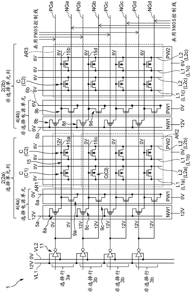
[0077] (1-1) Overall structure of nonvolatile semiconductor memory device

[0078] in with Figure 13 Corresponding parts are denoted by the same symbols figure 1 Here, 1 represents the nonvolatile semiconductor memory device of the present invention, which has a structure in which a plurality of cell columns 2 of the same structure are arranged in a row direction (left-right direction). Here, the structures of the plurality of cell columns 2 are the same, so the following description will focus on the cell column 2 of the first column. At this time, an N-type slot NW1, a P-type slot PW1, and a P-type storage slot PW2 are sequentially arranged on the cell column 2, and a power supply unit 4 is formed on the N-type slot NW1 and the P-type slot PW1. A plurality of memory cells C are formed in a matrix on the memory groove PW2.

[0079] In the power supply unit 4, a first power supply line 5a extending in the column direction (vertical direction) is formed on the N-type groove...

no. 2 approach

[0124] (2-1) Data writing operation

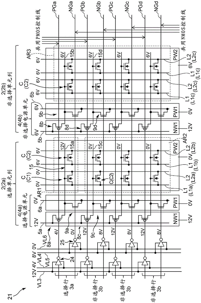
[0125] in the same figure 1 Corresponding parts are denoted by the same symbols figure 2 Among them, 21 represents the nonvolatile semiconductor storage device of the second embodiment. The difference between the second embodiment and the nonvolatile semiconductor storage device 1 of the first embodiment is that the nonvolatile semiconductor storage device 1 of the second embodiment Replacement in storage figure 1 The first MOS power line VL1 and the second MOS power line VL2 are provided with a first PMOS power line VL3, a second PMOS power line VL4, a first NMOS power line VL5, and a second NMOS power line VL6. Actually, the nonvolatile semiconductor storage device 21 has the following structure: the first PMOS power line VL3 and the second PMOS power line VL4 are extended in the column direction, parallel to the first PMOS power line VL3 and the second PMOS power line VL4 Likewise, the first NMOS power line VL5 and the second NMOS...

no. 3 approach

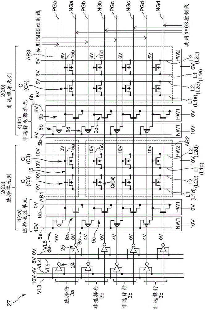
[0179] (3-1) Data writing operation

[0180] in with figure 2 Corresponding parts are denoted by the same symbols Figure 4 Among them, 31 denotes a nonvolatile semiconductor storage device according to the third embodiment. The difference between this nonvolatile semiconductor storage device 31 and the above-mentioned nonvolatile semiconductor storage device 21 according to the second embodiment is that not only PMOS switches 8a, 8c, ... (8b, 8d, ...) and NMOS switches 9a, 9c, ... (9b, 9d, ...), and also auxiliary NMOS switches 36a, 36c, ... (36b, 36d, ...) are provided on each power supply unit 34, and when data is written, in the non-selected cell column 32b, 0V is applied to each non-selected word line 15b, 15d, ... through the auxiliary NMOS switches 36b, 36d, ... Disable gate voltage.

[0181] Also, in the nonvolatile semiconductor memory device 31 according to the third embodiment, since it has such a structure, it is possible to turn on and off the PMOS switches 8a...


PUM


Abstract

Proposed is a non-volatile semiconductor storage device with which, while effecting miniaturization, it is possible to suppress a disturb occurrence better than before. In a non-volatile semiconductor storage device, forming a plurality of words in a matrix, disposing a power source unit for each word line column (memory well), imparting a different unit voltage to each power source unit corresponding to whether a selected memory well is present in a given word line column, switching on a word line unit basis a switch mechanism of each power source unit according to a control line voltage value, and individually imparting to each word line either a charge storage gate voltage or a charge storage interdiction gate voltage, it is possible to freely set for each word line column a charge storage interdiction gate voltage value or a bit line voltage value which is capable of suppressing a disturb occurrence. A plurality of power source units are connected to a common control line in the row direction, obviating the need for a separate address decoder for each word column line, and allowing effecting miniaturization.

Description

technical field [0001] The present application relates to a nonvolatile semiconductor memory device, and more particularly to a nonvolatile semiconductor memory device capable of writing data to predetermined memory cells among a plurality of memory cell transistors arranged in a matrix (hereinafter simply referred to as memory cells). device. Background technique [0002] In the prior art, as a nonvolatile semiconductor memory device, for example, a nonvolatile semiconductor memory device in which data is written by storing charges in a charge storage layer of a memory cell according to quantum tunneling is disclosed (for example, refer to Patent Document 1 and non-patent literature 1). it's here, Figure 13 Shown is a conventional nonvolatile semiconductor storage device 501, which has the following structure: including, for example, a plurality of P-type storage grooves W503a, W503b, W503c, and W503d arranged in the row direction (left-right direction), and each P-type s...

Claims


Application Information

Patent Timeline
Patent Type & Authority Applications(China)
IPC IPC(8): G11C16/06G11C16/02
CPCG11C16/08G11C16/24G11C16/12G11C16/0483G11C16/0466G11C16/0408G11C16/30G11C5/025G11C5/063G11C16/04G11C5/06
Inventor 葛西秀男品川裕谷口泰弘
Owner FLOADIA
Why Eureka
Try Eureka